
Datasheet

LTC4307-1
8
43071fa
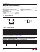
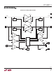
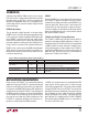
Figure 2. Input-Output Falling Edge Waveforms
OPERATION
INPUT SIDE
150pF
1V/DIV
OUTPUT SIDE
50pF
1V/DIV
200ns/DIV
43071 F02
Start-Up
When the LTC4307-1 fi rst receives power on its V
CC
pin
during power-up, it starts in an undervoltage lockout
(UVLO) state, ignoring any activity on the SDA or SCL
pins until V
CC
rises above 2V (typ). This is to ensure that
the LTC4307-1 does not try to function until it has enough
voltage to do so.
Once the LTC4307-1 comes out of UVLO, it monitors both
2-wire busses for either a stop bit or bus idle condition to
indicate the completion of data transactions. When both
sides are idle or one side has a stop bit condition while the
other is idle, the input-to-output connection circuitry is acti-
vated, joining SDAIN to SDAOUT and SCLIN to SCLOUT.
Connection Circuitry
Once the connection circuitry is activated, the functionality
of the SDAIN and SDAOUT pins is identical. A low forced
on either pin at any time results in both pin voltages being
low. The LTC4307-1 is tolerant of I
2
C bus DC logic low
voltages up to the 0.3V
CC
V
IL
I
2
C specifi cation.
When the LTC4307-1 senses a rising edge on the bus,
it deactivates its pull-down devices for bus voltages as
low as 0.48V. Care must be taken to ensure that devices
participating in clock stretching or arbitration force logic
low voltages below 0.48V at the LTC4307-1 inputs.
SDAIN and SDAOUT enter a logic high state only when
all devices on both SDAIN and SDAOUT release high.
The same is true for SCLIN and SCLOUT. This important
feature ensures that clock stretching, clock synchroniza-
tion, arbitration and the acknowledge protocol always
work, regardless of how the devices in the system are
tied to the LTC4307-1.
Another key feature of the connection circuitry is that it
provides bidirectional buffering, keeping the capacitances
of the two 2-wire busses isolated from each other. Plac-
ing an LTC4307-1 close to an HDMI port inside an HDMI
transmitter or receiver allows the HDMI device to pass
the capacitance compliance specifi cation. Because of this
isolation, the waveforms on SDAIN and SCLIN look slightly
different than the corresponding waveforms on SDAOUT
and SCLOUT as described here.
Input to Output Offset Voltage
When a logic low voltage, V
LOW1
, is driven on any of the
LTC4307-1’s data or clock pins, the LTC4307-1 regulates
the voltage on the opposite data or clock pins to a slightly
higher voltage, typically 60mV above V
LOW1
. This offset is
practically independent of pull-up current (see the Typical
Performance curves).
Propagation Delays
During a rising edge, the rise time on each side is de-
termined by the bus pull-up resistor and the equivalent
capacitance on the line. If the pull-up resistors are the
same, a difference in rise time occurs which is directly
proportional to the difference in capacitance between
the two sides. Users must account for differences in the
RC time constants between the two 2-wire busses and
ensure that all system timing specifi cations are met on
both busses.
There is a fi nite propagation delay through the connection
circuitry for falling waveforms. Figure 2 shows the falling
edge waveforms for V
CC
= 5.5V, a 10k pull-up resistor on
each side, 150pF parasitic capacitance on the input bus and
50pF on the output pins. An external N-channel MOSFET
device pulls down the voltage on the side with 150pF
capacitance; the LTC4307-1 pulls down the voltage on the
opposite side with a delay of 80ns. This delay is always
positive and is a function of supply voltage, temperature
and the pull-up resistors and equivalent bus capacitances
on both sides of the bus. The Typical Performance Charac-
teristics section shows propagation delay as a function of
temperature and voltage for 10k pull-up resistors and 50pF
equivalent capacitance on both sides of the part. Also, the
t
PHL
vs C
OUT
curve for V
CC
= 5.5V shows that increasing the