
Datasheet

LTC4307-1
9
43071fa
OPERATION
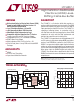
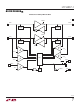
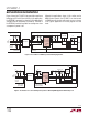
Figure 3 shows the LTC4307-1 in a capacitance buffering
application. Due to the LTC4307-1’s capacitance buffering
feature and sub-10pF input capacitance, this application
circuit passes the HDMI 50pF maximum DDC capacitance
specifi cation easily when the LTC4307-1 is located right at
the HDMI connector interface as shown. The capacitance
of the internal bus connected to the SDAIN and SCLIN
pins may be much larger than 50pF, but because of the
LTC4307-1’s capacitance buffering, the internal bus ca-
pacitance is isolated from the HDMI connector.
APPLICATIONS INFORMATION
In HDMI, the sink device pulls the hot plug detect HPD
signal high to tell the source that it is ready to accept
commands through the DDC. This signal can be controlled
through the READY pin of the LTC4307-1 to prevent the
possibility of erroneous attempts by the source to contact
the sink before the sink is ready to return its extended
display identifi cation data (EDID). The READY pin only
goes high after 5V is applied and the LTC4307-1 ENABLE
pin is pulled high by the HDMI receiver IC, a controller in
the sink, or the 5V line itself.
capacitance from 50pF to 150pF results in a t
PHL
increase
from 81ns to 91ns. Larger output capacitances translate
to longer delays (up to 125ns). Users must quantify the
difference in propagation times for a rising edge versus
a falling edge in their systems and adjust setup and hold
times accordingly.
READY Digital Output
This pin provides a digital fl ag which is low when either
ENABLE is low or the start-up sequence described earlier
in this section has not been completed. READY goes high
when ENABLE is high and the input and output 2-wire
busses are connected. The pin is driven by an open-drain
pull-down capable of sinking 3mA while holding 0.4V on
the pin. Connect a resistor to V
CC
to provide the pull-up.
READY can be used to control the HDMI hot plug detect
(HPD) signal to prevent the possibility of erroneous at-
tempts by the source to contact the sink before the sink
is ready to communicate.
ENABLE
When the ENABLE pin is driven below 0.8V with respect to
the LTC4307-1’s ground, the input 2-wire bus is discon-
nected from the output 2-wire bus and the READY pin is
internally pulled low. When the pin is driven above 2V,
the part waits for data transactions on both 2-wire bus-
ses to be complete (as described in the Start-Up section)
before connecting the two sides. At this time the internal
pull-down on READY releases.
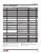
LTC4307 and LTC4307-1 Feature Differences
The LTC4307-1 HDMI level-shifting 2-wire bus buffer is
specifi cally intended for HDMI applications. Features in
the general purpose LTC4307 device that are not required
in HDMI systems have been removed. In addition, level-
shifting functionality has been added to the LTC4307-1
to allow 3.3V HDMI devices to interface safely to the 5V
HDMI DDC bus. See Table 1 for a list of the differences
between the LTC4307 and LTC4307 -1.
Table 1. Differences Between the LTC4307 and the LTC4307-1
SPECIFICATION LTC4307 LTC4307-1 COMMENTS ON LTC4307-1
Pre-charge Yes No HDMI DDC Lines are Not Hot Swapped
Level Shifting No
Yes,
2.2V to 5.5V
Provides Communication Between 3.3V and 5V DDC Busses,
Protects 3.3V Devices from 5V Supply
Stuck Bus Disconnect and Recovery Yes No Stuck Busses, Not an Issue in HDMI Systems
Rise Time Accelerators Yes No Complies with HDMI Specifi cation Version 1.3 DDC Capacitance
Requirement