
Datasheet

LTC4307
7
4307f
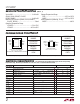
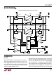
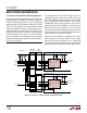
BLOCK DIAGRA
W
100k
PRECHARGE
PC_CONNECT
100k
0.55V
CC
0.55V
CC
1.4V
UVLO
100k
0.55V
CC
0.55V
CC
CONNECT
CONNECT
100k
8mA
I
BOOSTSDA
I
BOOSTSDA
SDAIN
6
SLEW RATE
DETECTOR
8mA
CONNECT
CONNECT
SLEW RATE
DETECTOR
8mA
I
BOOSTSCL
I
BOOSTSCL
SLEW RATE
DETECTOR
8mA
SLEW RATE
DETECTOR
CONNECT
SDAOUT
7
V
CC
8
SCLIN
3
CONNECT
SCLOUT
2
READY
5
PC_CONNECT
30ms
TIMER
LOGIC
ENABLE
PC_CONNECT
I
BOOSTSCL
I
BOOSTSDA
1
GND
4307 BD
4
95μs
DELAY
+
+
–
–
+
–
+
–
+
–
Low Offset 2-Wire Bus Buffer with Stuck Low Timeout
OPERATION
Start-Up
When the LTC4307 fi rst receives power on its V
CC
pin,
either during power-up or live insertion, it starts in an
undervoltage lockout (UVLO) state, ignoring any activity
on the SDA or SCL pins until V
CC
rises above 2V (typ).
This is to ensure that the LTC4307 does not try to function
until it has enough voltage to do so.
During this time, the 1V precharge circuitry is active and
forces 1V through 100k nominal resistors to the SDA
and SCL pins. Because the I/O card is being plugged
into a live backplane, the voltage on the backplane SDA
and SCL busses may be anywhere between 0V and V
CC
.
Precharging the SCL and SDA pins to 1V minimizes the
worst-case voltage differential these pins will see at the