
Datasheet

LTC4307
9
4307f
OPERATION
Bus Stuck Low Timeout
When SDAOUT or SCLOUT is low, an internal timer is
started. The timer is only reset by that respective input
going high. If it does not go high within 30ms (typical)
the connection between SDAIN and SDAOUT, and between
SCLIN and SCLOUT is broken. After at least 40μs, the
LTC4307 automatically generates up to 16 clock pulses
at 8.5kHz (typical) on SCLOUT in an attempt to unstick
the bus. When the clock pulses are completed, a stop bit
will be generated on SCLOUT and SDAOUT to reset any
circuity on that bus. When the low SDAOUT or SCLOUT
pin goes high, a connection is enabled waiting for a stop
bit or a bus idle to make a connection.
When powering up into a bus stuck low condition, the
connection circuitry joining the SDA and SCL busses on
the I/O card with those on the backplane is not activated
and is only reset when SDAOUT and SCLOUT are high.
30ms after UVLO, automatic clocking takes place as
described above.
READY Digital Output
This pin provides a digital fl ag which is low when either
ENABLE is low, the start-up sequence described earlier in
this section has not been completed, or the LTC4307 has
disconnected due to a stuck bus condition. READY goes
high when ENABLE is high and the backplane and card
sides are connected. The pin is driven by an open-drain
pull-down capable of sinking 3mA while holding 0.4V on
the pin. Connect a resistor to V
CC
to provide the pull-up.
ENABLE
When the ENABLE pin is driven below 0.8V with respect to
the LTC4307’s ground, the backplane side is disconnected
from the card side and the READY pin is internally pulled
low. When the pin is driven above 2V, the part waits for
data transactions on both the backplane and card sides to
be complete (as described in the Start-Up section) before
connecting the two sides. At this time the internal pull-
down on READY releases. When ENABLE is low, automatic
clocking is disabled.
A rising edge on ENABLE after a bus stuck low condition
has occurred forces a connection between SDAIN, SDAOUT,
and SCLIN, SCLOUT even if the bus stuck low condition
has not been cleared. At this time the 30ms timer is reset
but not disabled.
Rise Time Accelerators
Once connection has been established, rise time accelerator
circuits on all four SDA and SCL pins are enabled. During
positive bus transitions, the rise time accelerators provide
strong, slew-limited pull-up currents that make the bus
voltage rise at a rate of 100V/μs. The rise time accelerators
signifi cantly improve system reliability in two ways. First,
they provide smooth, controlled transitions during rising
edges for both small and large systems. Because the ac-
celerator pull-up impedance is signifi cantly lower than the
bus pull-up resistance, the system is much less susceptible
to noise on rising edges. Second, the accelerators allow
users to choose large bus pull-up resistors, reducing power
consumption and improving logic low noise margin.
For these reasons, it is strongly recommended that users
choose bus pull-up resistors so that the bus will rise on its
own at a rate of at least 0.8V/μs to guarantee activation of
the accelerators. The rise time accelerators are disabled
until the sequence of events described in the start-up sec-
tion has been completed. They are also disabled during
automatic clocking.
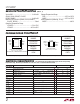
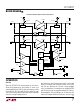
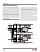
Figure 2. Input-Output Rising Edge Waveforms Figure 3. Input-Output Falling Edge Waveforms
OUTPUT SIDE
50pF
1V/DIV
INPUT SIDE
150pF
1V/DIV
200ns/DIV
4307 F02
INPUT SIDE
150pF
1V/DIV
OUTPUT SIDE
50pF
1V/DIV
200ns/DIV
4307 F03