
Datasheet
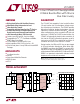


LTC4307
6
4307f
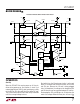
PI FU CTIO S
UUU
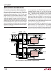
ENABLE (Pin 1): Connection Enable Input. This is a 1.4V
digital threshold input pin. For normal operation pull or tie
ENABLE high. Driving ENABLE below 0.8V isolates SDAIN
from SDAOUT, SCLIN from SCLOUT and asserts READY
low. A rising edge on ENABLE after a fault has occurred
forces a connection between SDAIN, SDAOUT and SCLIN,
SCLOUT. Connect to V
CC
if unused.
SCLOUT (Pin 2): Serial Clock Output. Connect this pin to
an SCL bus segment where stuck bus recovery is needed.
A pull-up resistor should be connected between this pin
and V
CC
.
SCLIN (Pin 3): Serial Clock Input. Connect this pin to an
SCL bus segment that needs to be isolated from stuck
bus problems. A pull-up resistor should be connected
between this pin and V
CC
.
GND (Pin 4): Device Ground. Connect this pin to a ground
plane for best results.
READY (Pin 5): Connection READY Status Output. The
READY pin is an open-drain N-channel MOSFET output that
pulls low when ENABLE is low, or when the start-up and
connection sequence described in the Operation section
has not been completed. READY also goes low when the
LTC4307 disconnects the inputs from the outputs due to
the bus being stuck low for at least 30ms. READY goes high
when ENABLE is high and a connection is made. Connect
a pull-up resistor, typically 10k, from this pin to V
CC
to
provide the pull-up. This pin can be fl oated if unused.
SDAIN (Pin 6): Serial Data Input. Connect this pin to an
SDA bus segment that needs to be isolated from stuck
bus problems. A pull-up resistor should be connected
between this pin and V
CC
.
SDAOUT (Pin 7): Serial Data Output. Connect this pin
to the SDA bus segment where stuck bus recovery is
needed. A pull-up resistor should be connected between
this pin and V
CC
.
V
CC
(Pin 8): Supply Voltage Input. Place a bypass capacitor
of at least 0.01μF close to V
CC
for best results.
Exposed Pad (Pin 9, DFN Package Only): Exposed Pad
may be left open or connected to device ground.