
Datasheet


LTC4308
4
4308f
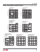
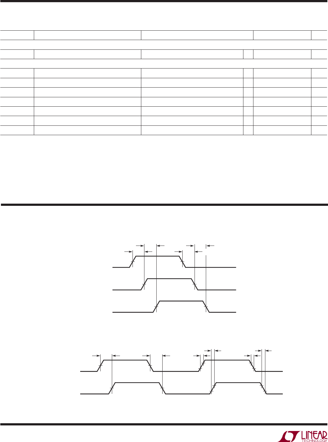
ENABLE, CONNECT, READY Timing
Rising and Falling Propagation Delays and Rise and Fall Times for SDAIN, SDAOUT and SCLIN, SCLOUT
Figure 1. Timing Diagrams
t
PLH_EN
ENABLE
CONNECT
READY
t
PLH_READY
t
PHL_READY
t
PHL_EN
4308 TD01
t
PLH
SDAIN/SCLIN
SDAOUT/SCLOUT
t
PHL
t
RISE
t
FALL
t
RISE
t
FALL
4308 TD02
TIMING DIAGRAMS
SYMBOL PARAMETER CONDITIONS MIN TYP MAX UNITS
Bus Stuck Low Timeout
t
TIMEOUT
Bus Stuck Low Timer SDAOUT = SCLOUT = 0V
l
25 30 35 ms
Timing Characteristics
f
I2C,MAX
I
2
C Maximum Operating Frequency (Note 3) 400 600 kHz
t
BUF
Bus Free Time Between Stop and Start Condition (Note 3) 1.3 μs
t
HD,STA
Hold Time After (Repeated) Start Condition (Note 3) 100 ns
t
SU,STA
Repeated Start Condition Set-Up Time (Note 3) 0 ns
t
SU,STO
Stop Condition Set-Up Time (Note 3) 0 ns
t
HD,DATI
Data Hold Time Input (Note 3) 0 ns
t
SU,DAT
Data Set-Up Time (Note 3) 100 ns
ELECTRICAL CHARACTERISTICS
Note 1: Stresses beyond those listed under Absolute Maximum Ratings
may cause permanent damage to the device. Exposure to any Absolute
Maximum Rating condition for extended periods may affect device
reliability and lifetime.
Note 2: See “Propagation Delays” in the Operations section for a
discussion of t
PHL
and t
PLH
as a function of pull-up resistance and bus
capacitance.
Note 3: Determined by design, not tested in production.
Note 4: Measure points are 0.3 • V
CC
and 0.7 • V
CC
.
Note 5: I
PULLUPAC
varies with temperature and V
CC
voltage as shown in the
Typical Performance Characteristics section.
Note 6: I
CC
test performed with connection circuitry active.
Note 7: All currents into pins are positive; all voltages are referenced to
GND unless otherwise specifi ed.
The l denotes the specifi cations which apply over the full operating
temperature range, otherwise specifi cations are at T
A
= 25°C. V
CC
= 3.3V, unless otherwise noted.