
Datasheet


LTC4309
11
4309fa
If the rise time accelerators are enabled, the bus pull-up
supply can be greater than or equal to V
CC
for the output
busses and accordingly, the input pull-up supply can
be greater than or equal to V
CC2
for the input busses.
This ensures the LTC4309’s rise time accelerators do
not source current through the pull-up resistors into the
pull-up supply. If the rise time accelerator circuitries are
disabled, the bus pull-up supply can be as low as 2V for
V
CC
≥ 2.9V and for V
CC
< 2.9V, the bus pull-up supply can
be as low as 1.7V. The bound on the lower supply limit
exists to ensure the bus signal range exceeds the logic
input threshold voltage, V
THR
.
Resistor Pull-Up Value Selection
To guarantee the rise time accelerators are activated during
a rising edge, the bus must rise on its own with a positive
slew rate of at least 0.8V/μs. To achieve this, choose a
maximum resistor value R
PULLUP
using the formula:
R
PULLUP
(V
BUS(MIN)
– 0.8V)• 1250
ns
V
C
BUS
Where R
PULLUP
is the pull-up resistor value in kilo ohms,
V
BUS(MIN)
is the minimum bus pull-up supply voltage and
C
BUS
is the equivalent bus capacitance in pico-Farads
(pF).
To estimate the value of C
BUS
, use a general rule of 20pF
of capacitance per device on the bus (10pF for the device
and 10pF for interconnect).
In addition, R
PULLUP
must be strong enough to overcome
the precharge voltage and provide logic highs on SDAOUT
and SCLOUT for the start-up and connection circuitry to
connect the backplane to the card. Regardless of the bus
capacitance, always choose
R
PULLUP
V
BUS(MAX)
–V
THR
100μA
to the pull-up impedance, multiple LTC4309 buffers can
be used in a single system. This allows the user to divide
the line and device capacitances into more sections with
buffering and meet rise and fall times.
The LTC4309 disconnects when both bus I/O’s are above
0.48V and rising. In systems with large ground bounce,
if many devices are cascaded, the 0.48V threshold can be
exceeded, and the transients associated with the ground
bounce can appear to be a rising edge. Under this condition,
the LTC4309 with inputs above 0.48V may disconnect.
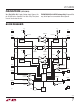
Level Shifting Applications
Systems requiring different supply voltages for the
backplane side and the card side can use the LTC4309
for bidirectional level shifting, as shown in Figure 6. The
LTC4309 can level shift between bus pull-up supplies as
low as 1.7V, with the accelerators disabled, to as high as
5.5V. Level shifting allows newer designs that require low
voltage supplies, such as EEPROMs and microcontrollers,
the capability to interface with legacy backplanes which
may be operating at higher supply voltages.
Systems with Supply Voltage Droop
In large 2-wire systems, the supply voltages seen by devices
at various points in the system can differ by a few hundred
millivolts or more. For proper operation, make sure that
the V
CC2(LTC4309)
is ≥ 1.8V, and V
CC(LTC4309)
≥ 2.3V.
Additional Pull-Up Supply Options
In typical applications, a pull-up resistor connected from
the LTC4309’s bus output pins to V
CC
and bus input pins
to V
CC2
or V
CC
, if V
CC2
is grounded, is suffi cient. However,
for unique applications, additional fl exibility is available for
bus pull-up supplies other than V
CC
or V
CC2
. One example
is shown in Figure 8. The expanded bus pull-up range is
dependent on the user confi guration of the rise time ac-
celerators and the supply voltage, V
CC
.
APPLICATIONS INFORMATION