
Datasheet

LTC4309
6
4309fa
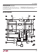
ENABLE (Pin 1/Pin1): Connection Enable Input. This 1.4V
digital threshold input pin enables or disables the LTC4309.
For normal operation pull or connect ENABLE high. Driving
ENABLE below the 0.8V threshold isolates SDAIN from
SDAOUT, SCLIN from SCLOUT, asserts READY low, and
prohibits automatic clock and stop bit generation during a
fault condition. A rising edge on ENABLE after a fault has
occurred forces a connection between SDAIN, SDAOUT
and SCLIN, SCLOUT. Connect to V
CC
if unused.
DISCEN (Pin 2/Pin 3 ): Bus Stuck Low Disconnect Enable
Input. This pin, when high, allows the stuck low bus
timeout circuitry to disconnect the bus in a fault condition.
When connected to GND, this pin disables the circuitry
that disconnects the bus under a fault condition; however,
the FAULT pin will still go low.
SCLOUT (Pin 3/Pin 4): Serial Clock Output. Connect this
pin to a SCL bus segment where bus stuck low recovery is
desired. If the output rise time accelerators are enabled, a
pull-up resistor should be connected between this pin and
a bus supply greater than or equal to V
CC
. Bus supplies
can be lower than V
CC
if the output rise time accelerators
are disabled. See Application Information section for
detailed bus pull-up supply options.
SCLIN (Pin 4/Pin 5): Serial Clock Input. Connect this pin
to a SCL bus segment where isolation from bus stuck
low issues is desired. If the input rise time accelerator is
enabled, a pull-up resistor should be connected between
this pin and a bus supply greater than or equal to V
CC2
.
Bus supplies can be lower than V
CC2
if the input rise time
accelerators are disabled. See Application Information
section for detailed bus pull-up supply options.
ACC (Pin 5/Pin 6): Rise Time Accelerator Control Input.
This nominal 0.7V threshold input pin enables and disables
all rise time accelerators on the SDA and SCL pins. Connect
ACC to GND to enable all four rise time accelerators or
connect ACC to V
CC
to disable all four rise time accelerators.
Connect ACC to V
CC2
to GND to enable the accelerators
on SDAOUT and SCLOUT only.
GND (Pin 6/Pin 8): Device Ground. Connect this pin to a
ground plane for best results.
READY (Pin 7/Pin 9): Connection Ready Status Output.
This open-drain N-channel MOSFET pin pulls low when
ENABLE is low, when the start-up and connection sequence
described in the Operation section has not been completed,
or when the LTC4309 disconnects the input and output
pins due to a bus stuck low condition. READY goes high
when ENABLE is high and connection is made between the
input and output pins. Connect a pull-up resistor, typically
10k, from this pin to the bus pull-up supply. This pin can
be left open if unused.
FAULT (Pin 8/Pin 11): Bus Stuck Low Timeout Output. This
open drain N-channel MOSFET output pulls low after 30ms
when there is a bus stuck low condition on the output pins
of the LTC4309. In normal operation FAULT is high. Connect
a pull-up resistor, typically 10k, from this pin to the bus
pull-up supply. This pin can be left open if unused.
SDAIN (Pin 9/Pin 12): Serial Clock Input. Connect this
pin to a SDA bus segment where isolation from bus stuck
low issues is desired. If the input accelerator is enabled, a
pull-up resistor should be connected between this pin and
a bus supply greater than or equal to V
CC2
. Bus supplies
can be lower than V
CC2
if the input rise time accelerators
are disabled. See Application Information section for
detailed bus pull-up supply options.
SDAOUT (Pin 10/Pin 13): Serial Clock Output. Connect this
pin to a SCL bus segment where bus stuck low recovery is
desired. If the output rise time accelerators are enabled, a
pull-up resistor should be connected between this pin and
a bus supply greater than or equal to V
CC
. Bus supplies
can be lower than V
CC
if the output rise time accelerators
are disabled. See Application Information section for
detailed bus pull-up supply options.
V
CC2
(Pin 11/Pin 14): Supply Voltage Input for SDAIN and
SCLIN Rise Time Accelerator Circuitry. V
CC2
supplies the
rise time accelerator circuitry on the input side. Bypass
this pin to GND with a capacitor of at least 0.01μF and
place close to V
CC2
for best results. If V
CC2
is connected
to GND, the input side rise time accelerator circuitry is
disabled, regardless of ACC.
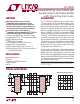
(DE12/GN16)
PIN FUNCTIONS