
Datasheet

LTC4309
8
4309fa
Start-Up
When the LTC4309 fi rst receives power on its V
CC
pin,
either during power up or live insertion, it starts in an under
voltage lockout (UVLO) state, ignoring any activity on the
SDA or SCL pins until V
CC
rises above 2V. This ensures
the LTC4309 does not try to function until enough supply
voltage is present.
During this time, the 1V precharge circuitry is actively
forcing 1V through 100k nominal resistors to the SDA
and SCL pins. Because the I/O card is being plugged
into a live backplane, the voltage on the backplane SDA
and SCL busses may be anywhere between 0V and V
CC
.
Precharging the SCL and SDA pins to 1V minimizes the
worst-case voltage differential these pins will see at the
moment of contact, therefore minimizing the amount of
disturbance caused by the I/O card.
Once the LTC4309 exits from UVLO, it monitors both the
input and output pins for either a stop bit or a bus idle
condition to indicate the completion of data transactions.
When both sides are idle or one side has a stop bit while
the other is idle, the connection circuitry is activated,
joining the SDA and SCL busses on the input side with
those on the output side.
Rise Time Accelerators
Once connection has been established if ACC is connected
to ground and V
CC2
is powered from a supply voltage greater
than or equal to 1.8V, the rise time accelerator circuits on
all four SDA and SCL pins are enabled. During positive bus
transitions of at least 0.8V/μs, the rise time accelerators
provide strong, slew-limited pull-up currents to force the
bus voltage to rise at a rate of 100V/μs. Enabling the rise
time accelerators allows users to choose larger bus pull-
up resistors, reducing power consumption and improving
logic low noise margins, or design with bus capacitances
beyond those specifi ed in the I
2
C specifi cations.
To ensure the rise time accelerators are properly activated
when the rise time accelerators are enabled, users should
choose bus pull-up resistors that guarantee the bus will
rise on its own at a rate of at least 0.8V/μs. See the Ap-
plication Information section for determining the correct
pull-up resistor size.
All four rise time accelerators can be disabled by connect-
ing ACC to V
CC
. To activate the rise time accelerators on
only SDAOUT and SCLOUT, connect both ACC and V
CC2
to ground. The rise time accelerators are also internally
disabled until the sequence of events described in the
start-up section have been completed, as well as during
automatic clocking and stop bit generation for a bus stuck
low recovery event.
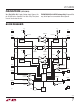
Connection Circuitry
Once the connection circuitry is activated, the functionality
of the input and output bus of the respective SDA or SCL
pins are identical. A low forced on either output or input
pin at any time results in both pin voltages forced low.
The LTC4309 is tolerant of I
2
C bus DC logic low voltages
up to the V
IL
specifi cation of 0.3 • V
CC
.
When the LTC4309 senses a rising edge on the bus, with
a slew rate greater than 0.8V/μs, the internal pull-down
device for the respective bus is deactivated at bus volt-
ages as low as 0.48V. This methodology maximizes the
effectiveness of the rise time accelerator circuitry and
maintains compatibility with other devices in the LTC4300
bus buffer family. Care must be taken to ensure devices
participating in clock stretching or arbitration are capable
of forcing logic low voltages below 0.48V at the LTC4309’s
SDA and SCL pins.
A high occurs when all devices on the input and output
pins release high. These important features ensures the
I
2
C specifi cation protocols such as clock stretching, clock
synchronization, arbitration, and acknowledge function
seamlessly in all cases as specifi ed, regardless of how the
devices in the system are connected to the LTC4309.
Another key feature provided by the connection circuitry
is input and output bus capacitance isolation through
bidirectional buffering. Because of this isolation, the
waveforms on the input busses look slightly different than
the corresponding output bus waveforms, as described
below.
Input to Output Offset Voltage
When a logic low voltage is driven on any of the LTC4309’s
data or clock pins, the LTC4309 regulates the voltage on
the other side of the device to a slightly higher voltage,
OPERATION