
Datasheet


LTC4309
4
4309fa
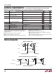
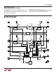
TIMING DIAGRAMS
ENABLE and READY Timing
t
PLH_EN
ENABLE
CONNECT
READY
t
PLH_READY
t
PHL_READY
t
PHL_EN
4309 TD01
SDA/SCL Propagation Delays, Rise and Fall Times
t
PLH
SDAIN/SCLIN
SDAOUT/SCLOUT
t
PHL
t
RISE
t
FALL
t
RISE
t
FALL
4309 TD02
Figure 1. Timing Diagrams
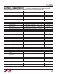
SYMBOL PARAMETER CONDITIONS MIN TYP MAX UNITS
V
THR(HYST)
SDA, SCL Logic Input Threshold Voltage
Hysteresis
(Note 3) 50 mV
C
IN
Digital Input Capacitance SDAIN,
SDAOUT, SCLIN, SCLOUT
(Note 3) 10 pF
I
LEAK
Input Leakage Current SDA, SCL, ACC, DISCEN Pins
l
±5 μA
V
OL
Output Low Voltage SDA, SCL Pins, I
SINK
= 4mA, Driven SDA/SCL = 0.2V, V
CC
=
V
CC2
= 2.7V
l
0 0.4 V
2.7k to V
CC
on SDA, SCL, Driven SDA/SCL = 0.1V,
V
CC
= V
CC2
= 3.3V
l
120 170 205 mV
V
ILMAX
Buffer Input Logic Low Voltage
l
1.2 V
Bus Stuck Low Timeout
t
TIMEOUT
Bus Stuck Low Timer SDAOUT, SCLOUT = OV
l
25 30 35 ms
V
OL_FAULT
FAULT Output Low Voltage I
FAULT
= 3mA
l
0.4 V
I
OFF_FAULT
FAULT Off Leakage Current
l
0.1 ±5 μA
The l denotes the specifi cations which apply over the full operating
temperature range, otherwise specifi cations are at T
A
= 25°C. V
CC
= 3.3V, V
CC2
= 3.3V, unless otherwise noted.
Note 1: Stresses beyond those listed under Absolute Maximum Ratings
may cause permanent damage to the device. Exposure to any Absolute
Maximum Rating condition for extended periods may affect device
reliability and lifetime.
Note 2: Test performed with connection circuity active.
Note 3: Determined by design, not subject to test.
Note 4: For larger equivalent bus capacitance, the skew increases, and
setup and hold times must be adjusted accordingly. Please see the
Operation Section of the datasheet.
Note 5: Measure points are 0.3 • V
CC
and 0.7 • V
CC
.
Note 6: All currents into pins are positive, all voltages are referenced to
GND, unless otherwise specifi ed.
Note 7: I
PULLUPAC
varies with temperature and V
CC
voltage as shown in the
Typical Performance Characteristics section.
ELECTRICAL CHARACTERISTICS