
Datasheet


LTC4312
10
4312f
APPLICATIONS INFORMATION
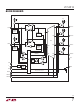
Figure 3. Connection of the LTC4312 in a Level Shift Application. V
CC2
Is
Less Than or Equal to the Minimum Bus Supply Voltage on the Output Side
If V
CC2
is tied low, the output side rise time accelerators
are disabled independent of the state of the ACC pin.
ACC tied high disables input and output RTAs. Using a
combination of the ACC pin and the V
CC2
voltage allows
the user independent control of the input and output side
rise time accelerators. The rise time accelerators are also
internally disabled during power-up and V
CC2
transitions,
as described in the Operation section, as well as during
automatic clocking and stop bit generation for a bus stuck
low recovery event.
The rise time accelerators when activated pull the bus up
to 0.9•V
CC
on the input side of the SDA and SCL lines.
On the output side the SDAOUT and SCLOUT lines are
pulled up by the rise time accelerators to 0.8•V
CC2
. For
V
CC2
voltages approaching 2.3V, acceleration of the output
bus may not be seen all the way to 0.8•V
CC2
due to the
threshold voltage of the NFET pass device.
Supply Voltage Considerations in Level Translation
Applications
Care must be taken to ensure that the bus supply voltages
on the input and output sides are greater than 0.9•V
CC
and
0.8•V
CC2
, respectively, to ensure that the bus is not driven
above the bus supplies by the rise time accelerators. This
is usually accomplished in a level shifting application by
tying V
CC
to the input bus supply and V
CC2
to the minimum
bus supply on the output side as shown in Figure 3.
If V
CC2
is grounded, the multiplexer pass gates are powered
from V
CC
. In this case the minimum output bus supply
of the enabled channels should be greater than or equal
to V
CC
to prevent cross-conduction between the enabled
output channels. This is shown in Figure 4. Grounding V
CC2
as shown in Figure 4 disables the output side rise time
accelerators independent of the state of the ACC pin. The
input rise time accelerators in this confi guration continue
to be controlled by the ACC pin and can be enabled inde-
pendently. In Figure 4, ACC is left open to obtain a high V
IL
and a 3mA rise time accelerator current on the input side.
LTC4312
GND
V
CC
V
CC2
4312 F03
SCLOUT1
SDAOUT1
SCLOUT2
SDAOUT2
SCLOUT1
SDAOUT1
SCLOUT2
SDAOUT2
SCLIN
SDAIN
ENABLE1
ENABLE2
ACC
DISCEN
FAULT
SCLIN
SDAIN
ENABLE1
ENABLE2
3.3V
FAULT
R3
10k
R2
10k
R1
10k
C1
0.01μF
3.3V 3.3V
R5
10k
R4
10k
C2
0.01μF
5V
R7
10k
R6
10k