
Datasheet

LTC4312
11
4312f
APPLICATIONS INFORMATION
Pull-Up Resistor Value Selection
To guarantee that the rise time accelerators are activated
during a rising edge, the bus must rise on its own with
a positive slew rate of at least 0.4V/μs. To achieve this,
choose a maximum R
BUS
using equation 1:
R
BUS
(Ω)≤
V
DD,BUS(MIN)
− V
RTA(TH)
()
0.4
V
µs
•C
BUS
(1)
R
BUS
is the bus pull-up resistor, V
DD, BUS(MIN)
the minimum
bus pull-up supply voltage, V
RTA(TH)
the voltage at which
the rise time accelerator turns on, which is a function of
ACC, and C
BUS
the equivalent bus capacitance. R
BUS
values
on each output channel must also be chosen to ensure
that when all the required output channels are enabled, the
total bus current is ≤4mA. The bus current in each output
channel can be 4mA if only one output channel is enabled
at any given time. The R
BUS
value on the input side must
also be chosen to limit the bus current to be ≤4mA. The
bus current for a single bus is determined by equation 2:
I
BUS
(A)=
V
DD,BUS
− 0.4V
R
BUS
(2)
Input to Output Offset Voltage and Propagation Delay
The LTC4312 introduces both an offset as well as a
propagation delay for falling edges between the input and
output. When a logic low voltage of ≥200mV is driven
on any of the LTC4312’s data or clock pins, the LTC4312
regulates the voltage on the opposite side to a slightly
higher value. When SCLIN or SDAIN is driven to a logic
low voltage, SCLOUT or SDAOUT is driven to a slightly
higher voltage as directed by equation 3 which uses SDA
as an example:
V
SDAOUT
(V)= V
SDAIN
+ 45mV
+ (10Ω + R
MUX
)•
V
DD,BUS
R
BUS
(3)
V
DD,BUS
is the output bus voltage, R
BUS
the output bus
pull-up resistance and R
MUX
is the resistance of the channel
transmission gate in the multiplexer shown in the block
diagram. The offset is affected by the V
CC2
voltage and bus
current. A higher V
CC2
voltage (V
CC
if V
CC2
is grounded)
reduces R
MUX
leading to a lower offset. See the Typical
Performance Characteristics plots for the variation of R
MUX
as a function of V
CC2
and temperature. When SDAOUT or
SCLOUT is driven to a logic low voltage ≥ 200mV, SCLIN
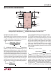
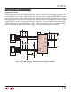
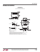
Figure 4. Connection of the LTC4312 in a Level Shift Application. V
CC
Is Less Than or Equal to the Minimum
Bus Supply Voltages on the Output Side. V
CC2
Is Grounded to Disable Output Rise Time Accelerators
LTC4312
GND
V
CC
V
CC2
4312 F04
SCLOUT1
SDAOUT1
SCLOUT2
SDAOUT2
SCLOUT1
SDAOUT1
SCLOUT2
SDAOUT2
SCLIN
SDAIN
ENABLE1
ENABLE2
ACC
DISCEN
FAULT
SCLIN
SDAIN
ENABLE1
ENABLE2
3.3V
FAULT
R3
10k
R2
10k
R1
10k
C1
0.01μF
C2
0.01μF
3.3V 3.3V
R5
10k
R4
10k
5V
R7
10k
R6
10k