
Datasheet

LTC4312
12
4312f
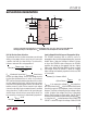
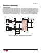
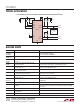
Figure 5. Cascading LTC4312s with Other LTC4312s and LTC Bus Buffers. Only the SDA Path Is Shown for Simplicity
or SDAIN is regulated to a logic low voltage as directed
by equation 4 which uses SDA as an example:
V
SDAIN
(V)= V
SDAOUT
+ 45mV +10Ω •
V
DD,BUS
R
BUS
(4)
The SCLOUT/SDAOUT to SCLIN/SDAIN offset is lower
than the reverse case as the multiplexer transmission gate
does not affect this offset. For driven logic low voltages
< 200mV, the above equations do not apply as the saturation
voltage of the open collector output transistor results in a
higher offset. However, the offset is guaranteed to be less
than 400mV for a total bus pull-up current of 4mA under
all conditions. See the Typical Performance Characteristics
curves for the buffer offset voltage as a function of the
driven logic low voltage and bus pull-up current.
The high-to-low propagation delay arises due to both the
fi nite response time of the buffers and their fi nite current
sink capability. See the Typical Performance Characteristics
curves for the propagation delay as a function of the bus
capacitance.
APPLICATIONS INFORMATION
Cascading LTC4312 Devices and Other LTC Bus Buffers
Multiple LTC4312s can be cascaded or the LTC4312 may
be cascaded with other LTC bus buffers as required by the
application. This is shown for the data pathway in Figure 5
where an LTC4312 is cascaded with other LTC4312s and
some select LTC bus buffers. The clock path is identical.
When using such cascades, users should be aware of the
additive logic low offset voltages (V
OS
) when determin-
ing system noise margin. If the sum of the offsets (refer
to Equations 3 and 4 and to the data sheets of the cor-
responding bus buffers) plus the worst-case driven logic
low voltage across the cascade exceeds the buffer turn off
voltage, signals will not be propagated across the cascade.
Also the minimum rise time accelerator (RTA) turn-on volt-
age (wherever applicable) of each device in the cascade
should also be greater than the maximum buffer turn-off
voltage of all the devices in the cascade. This condition
is required to prevent contention between one device’s
buffer and another’s RTA. Based on this requirement,
LTC4312
GND
3.3V
R1
10k
C1
0.01μF
V
CC
V
CC2
4312 F05
SDAOUT1
SDAOUT2
SDAIN
ACC
3.3V
LTC4312
V
CC
V
CC2
SDAOUT1
SDAOUT2
SDAIN
ACC
LTC4301
GND
V
CC
SDAOUTSDAIN
5V
LTC4312
GND
3.3V
C2
0.01μF
V
CC
V
CC2
SDAOUT1
SDAOUT2
SDAIN
ACC
C3
0.01μF
R2
10k
R3
10k
R4
10k
C4
0.01μF
C5
0.01μF
R5
10k
R6
10k
5V
3.3V
R7
10k
SDAOUT1
SDAOUT2
SDAOUT3
SDAOUT4
SDAOUT5
LTC4303
V
CC
SDAOUTSDAIN
5V
R8
10k
LTC4307
V
CC
SDAOUTSDAIN
5V
R9
10k
GND
GND
GND