
Datasheet

LTC4312
16
4312f
APPLICATIONS INFORMATION
LTC4312
GND
V
CC
V
CC2
4312 F10
SCLOUT1
SDAOUT1
SCLOUT2
SDAOUT2
SCLIN
SDAIN
ENABLE1
ENABLE2
ACC
DISCEN
FAULT
ENABLE1
ENABLE2
3.3V
FAULT
R3
10k
R2
10k
R1
10k
C1
0.01μF
C2
0.01μF
3.3V 3.3V
R5
10k
R4
10k
5V
R7
10k
R6
10k
I
2
C
DEVICE
V
OL
= 0.6V
I
2
C
DEVICE
IO CARD
CONNECTOR
I
2
C
DEVICE
IO CARD
CONNECTOR
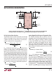
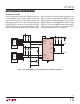
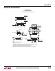
Figure 10. SDA, SCL Hot Swap™ and Operation with a Non-Compliant I
2
C Device
Hot-Swapping
Figure 10 shows the LTC4312 in a typical hot-swapping
application where the LTC4312 is on the backplane and I/O
cards plug into the downstream channels. The outputs must
idle high and the corresponding output channel must be
disabled before an I/0 card can be plugged or unplugged
from an output channel. Figure 10 also shows the use of
a non-compliant I
2
C device with the LTC4312. The high
noise margin of the LTC4312 supports logic low levels up
to 0.3 • V
CC
, allowing devices to drive greater than 0.4V
logic low levels on the clock and data lines.