
Datasheet
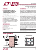


LTC4312
4
4312f
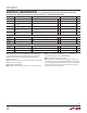
ELECTRICAL CHARACTERISTICS
The l denotes the specifi cations which apply over the full operating
temperature range, otherwise specifi cations are at T
A
= 25°C. V
CC
= V
CC2
= 3.3V unless otherwise noted.
SYMBOL PARAMETER CONDITIONS MIN TYP MAX UNITS
I
LEAK
Input Leakage Current DISCEN = ENABLE1-2 = 5.5V
l
0.1 ±10 μA
I
ACC(IN, HL)
ACC High, Low Input Current V
CC
= 5V, V
ACC
= 5V, 0V
l
±23 ±40 μA
I
ACC(IN, Z)
Allowable Leakage Current in
Open State
V
CC
= 5V
l
±5 μA
I
ACC(EN, Z)
ACC High Z Input Current V
CC
= 5V
l
±5 μA
V
ACC(L, TH)
ACC Input Low Threshold
Voltages
V
CC
= 5V
l
0.2•V
CC
0.3•V
CC
0.4•V
CC
V
V
ACC(H,TH)
ACC Input High Threshold
Voltages
V
CC
= 5V
l
0.7•V
CC
0.8•V
CC
0.9•V
CC
V
Stuck Low Timeout Circuitry
t
TIMEOUT
Bus Stuck Low Timer SDAOUT or SCLOUT < 0.3•V
CC
l
35 45 55 ms
V
FAULT(OL)
FAULT Output Low Voltage I
FAULT
= 3mA
l
0.4 V
I
FAULT(OH)
FAULT Leakage Current
l
0.1 ±5 μA
I
2
C Interface Timing
f
SCL(MAX)
I
2
C Frequency Max (Note 6)
l
400 kHz
t
PDHL
SDA, SCL Fall Delay V
CC
= 3V to 5.5V, C
BUS
= 50pF, I
BUS
= 1mA (Note 6) 60 100 ns
t
f
SDA, SCL Fall Times V
CC
= 3V to 5.5V, C
BUS
= 50pF, I
BUS
= 1mA (Note 6) 10 ns
Note 1: Stresses beyond those listed under Absolute Maximum Ratings
may cause permanent damage to the device. Exposure to any Absolute
Maximum Rating condition for extended periods may affect device
reliability and lifetime.
Note 2: All currents into pins are positive and all voltages are referenced to
GND unless otherwise indicated.
Note 3: SDAIN, SCLIN pulled low.
Note 4: V
MIN
= minimum of V
CC
and V
CC2
if V
CC2
> 2.25V else V
MIN
= V
CC
.
Note 5: V
IL
is tested for the following (V
CC
, V
CC2
) combinations:
(2.9V, 5.5V), (5.5V, 2.25V), (3.3V, 3.3V) and (5V, 0V).
Note 6: Guaranteed by design and not tested.
Note 7: Measured in a special DC mode with V
SDA,SCL
= V
RTA(TH)
+ 1V.
The transient I
RTA
seen during rising edges when ACC is low will depend
on the bus loading condition and the slew rate of the bus. The LTC4312’s
internal slew rate control circuitry limits the maximum bus rise rate to
75V/μs by controlling the transient I
RTA
.