
Datasheet


LTC4312
8
4312f
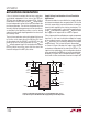
OPERATION
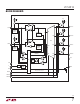
The Block Diagram shows the major functional blocks of the
LTC4312. The LTC4312 is a 1:2 multiplexer with capacitance
buffering for I
2
C signals. Capacitance buffering is achieved
by use of back to back buffers on the clock and data chan-
nels which isolate the SDAIN and SCLIN capacitances from
the SDAOUT and SCLOUT capacitances respectively. All
SDA and SCL pins are fully bidirectional. The high noise
margin allows the LTC4312 to operate with I
2
C devices
that drive a non-compliant high V
OL
. Multiplexing is done
using N-channel MOSFETs that are controlled by dedicated
ENABLE pins. When enabled, rise time accelerator pull-up
currents I
RTA
turn on during rising edges to reduce sys-
tem rise time. In a typical application the input side bus
is pulled up to V
CC
and the output side busses are pulled
up to V
CC2
although these are not requirements. V
CC
is
the primary power supply to the LTC4312. V
CC
and V
CC2
serve as the input and output side rise time accelerator
supplies respectively. Grounding V
CC2
disables the output
side accelerators. The multiplexer N-channel MOSFET
gates of the enabled channels are driven to V
CC2
if V
CC2
is > 1.8V, otherwise they are driven to V
CC
.
When the LTC4312 fi rst receives power on its V
CC
pin, it
starts out in an undervoltage lockout mode (UVLO) until
110μs after V
CC
exceeds 2.3V. During this time, the buffers
and rise time accelerators are disabled, the multiplexer
gates are off and the LTC4312 ignores transitions on the
clock and data pins independent of the state of the ENABLE
pins. V
CC2
transitions from a high to a low or vice-versa
across a 1.8V threshold also cause the LTC4312 to dis-
able the buffers, rise time accelerators and transmission
gates and to ignore the clock and data pins until 110μs
after that transition. Assuming that the LTC4312 is not in
UVLO mode, when one or both ENABLEs are asserted,
the LTC4312 activates the connection circuitry between
the SDAIN/SCLIN inputs and selected output channels.
The input rise time accelerators and the output rise time
accelerators of the selected channels are also enabled at
this time. When a SDA/SCL input pin or output pin on an
enabled output channel is driven below the V
IL,FALLING
level of 0.33 •V
MIN
, the buffers are turned on and the
logic low level is propagated though the LTC4312 to
the other side. For V
CC2
> 1.8V, V
MIN
is the lower of the
V
CC
and V
CC2
voltages. For V
CC2
< 1.8V, V
MIN
is the V
CC
voltage. The LTC4312 is designed to sink a minimum
total bus current I
OL
of 4mA while holding a V
OL
of 0.4V.
If multiple output channels are enabled, the bus current of
all enabled channels needs to be summed to get the total
bus current. See the Typical Performance Characteristics
curves for I
OL
as a function of temperature.
A high occurs when all devices on the input and output
sides release high. Once the bus voltages rise above the
V
IL, RISING
level, which is determined by the state of the ACC
pin, the buffers are turned off. The rise time accelerators
are turned on at a slightly higher voltage. The rise time
accelerators accelerate the rising edges of the SDA/SCL
inputs and selected outputs up to voltages of 0.9•V
CC
and
0.8•V
CC2
respectively, provided that the busses on their
own are rising at a minimum rate of 0.2V/μs as determined
by the slew rate detectors. ACC is a 3-state input that con-
trols V
IL,RISING
, the rise time accelerator turn-on voltage
and the rise time accelerator pull-up strength.
The LTC4312 detects a bus stuck low (fault) condition
when both clock and data busses are not simultaneously
high at least once in 45ms. The voltage monitoring for a
stuck low condition is done on the common internal node
of the clock and data outputs. Hence a stuck low condition
is detected only if it occurs on an enabled output channel.
When a stuck bus occurs, the LTC4312 asserts the FAULT
fl ag. If DISCEN is tied high, the LTC4312 also disconnects
the input and output sides. After waiting at least 40μs, it
generates up to sixteen 5.5kHz clock pulses on the enabled
SCLOUT pins and a stop bit to attempt to free the stuck
bus. If the bus recovers high before 16 clocks are issued,
the LTC4312 ceases issuing clocks and generates a stop
bit. If DISCEN is tied low, a stuck bus event only causes
FAULT fl ag assertion. Disconnection of the input and output
sides and clock generation do not occur. Once the stuck
bus recovers and the fault has been cleared, in order for a
connection to be established between the input and output
sides, both ENABLE pins need to be driven low followed
by the assertion high of the desired ENABLE pins. When
powering into a stuck low condition, the LTC4312 upon
exiting UVLO will connect the input and output sides for
45ms until a stuck bus timeout event is detected.