
Datasheet

LTC4313-1/LTC4313-2/
LTC4313-3
11
4313123f
applicaTions inForMaTion
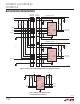
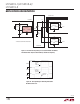
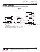
Live Insertion and Capacitance Buffering Application
Figure 5 illustrates an application of the LTC4313 that takes
advantage of the LTC4313’s Hot Swap, capacitance buffer-
ing and precharge features. If the I/O cards were plugged
directly into the backplane without LTC4313 buffers, all of
the backplane and card capacitances would directly add
together, making rise time requirements difficult to meet.
Placing an LTC4313 on the edge of each card isolates the
card capacitance from the backplane. For a given I/O card,
the LTC4313 drives the capacitance of everything on the
card and the devices on backplane must drive only the
small capacitance of the LTC4313 which is < 10pF.
In Figure 5 a staggered connector is used to connect the
LTC4313 to the backplane. V
CC
and GND are the longest
pins to ensure that the LTC4313 is powered and forcing
a 1V precharge voltage on the medium length SDA and
SCL pins before they contact the backplane. The 1V pre-
charge voltage is applied to the SDA and SCL pins through
200k resistors. Since cards are being plugged into a live
backplane whose SDA and SCL busses could be at any
voltage between 0 and V
CC
, precharging the LTC4313’s
SDA and SCL pins to 1V minimizes disturbances to the
backplane bus when cards are being plugged in. The low
(< 10pF) input capacitance of the LTC4313 also contributes
to minimizing bus disturbance as cards are being plugged
in. With ENABLE being the shortest pin and also pulled to
GND by a resistor, the staggered approach provides ad-
ditional time for transients associated with live insertion to
settle before the LTC4313 can be enabled. A 10k or lower
pull-down resistor from ENABLE to GND is recommended.
If a connector is used where all pins are of equal length,
the benefit of the precharge circuit is lost. Also, the
ENABLE signal to the LTC4313 must be held low until all
the transients associated with card insertion into a live
system die out.
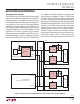
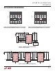
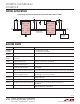
Level Translating to Voltages < 2.9V (LTC4313-3 Only)
The LTC4313-3 can be used for level translation to bus
voltages below 2.9V. Since the maximum buffer turn-on
and turn-off voltages are 0.36•V
CC
, the minimum bus
supply voltage is determined by the following equation,
V
DD,BUS(MIN)
≥
0.36 • V
CC
0.7
(4)
in order to meet the V
IH
= 0.7 • V
DD,BUS
requirement and
not impact the high side noise margin. Users willing to live
with a lower logic high noise margin can level translate
down to 1.4V. An example of voltage level translation from
3.3V to 1.8V is illustrated in Figure 6, where a 3.3V input
voltage bus is translated to a 1.8V output voltage bus.
Tying V
CC
to 3.3V satisfies Equation 4. A similar voltage
translation can also be performed going from a 3.3V bus
supply on the output side to a 1.8V input if the V
CC
pin of
the LTC4313-3 is tied to the 3.3V output supply.