
Datasheet

LTC4313-1/LTC4313-2/
LTC4313-3
15
4313123f
applicaTions inForMaTion
First, when two or more buffers are connected in a cas-
cade configuration, if the sum of the offsets across the
cascade (refer to Equation 3 and the data sheets of the
corresponding buffers) plus the worst-case driven logic
low voltage exceeds the minimum buffer turn-off voltage,
signals will not be propagated across the cascade. The
maximum driven logic low voltage must be set accordingly,
for correct operation in such cascades.
Second, noise margin is affected by cascading the LTC4313
with buffers whose RTA turn-on voltage is lower than the
LTC4313 buffer turn-off voltage. The V
IL
for the LTC4313
is set to 0.3 • V
CC
to achieve high noise margin provided
that the LTC4313 buffers do not contend with RTAs of
other products. To maximize logic low noise margin, dis-
able the RTAs of the other LTC buffers if possible and use
the RTAs of the LTC4313 in cascading applications. To
permit interoperability with other LTC buffers whose RTAs
cannot be disabled, the LTC4313 senses the RTA current
and turns off its buffers below 0.3 • V
CC
. This eliminates
contention between the LTC4313 buffers and other RTAs,
making the SDA/SCL waveforms monotonic.
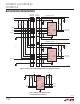
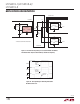
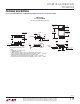
Figures 9 shows the LTC4313-1 operating on a bus shared
with LTC4300A and LTC4307 buffers. The correspond-
ing SCL waveforms are shown in Figure 10. The RTAs
on the LTC4300A and the LTC4307 cannot be disabled.
The backplane in Figure 9 has five I/O cards connected
to it. Each I/O card has a LTC bus buffer on its outside
edge for SDA/SCL Hot Swap onto the backplane. In this
example, there are three LTC4300As, one LTC4307 and
one LTC4313-1. The SCL1 bus is driven by an I
2
C master
(master not shown). When the SCL2 voltage crosses 0.6V
and 0.8V, the RTAs on the LTC4300A and LTC4307 turn on
respectively and source current into SCL2. The LTC4313-1
detects this and turns off its buffers, releasing SCL1 and
SCL2 high. Contention between the LTC4313-1 buffers
and the LTC4300A and LTC4307 RTAs is prevented and
the SCL1, SCL2 and SCL3 waveforms in Figure 10 are
monotonic. The logic low noise margin is reduced because
the LTC4313-1 buffers turn off when the SCL1 voltage is
approximately 0.6V.
Generally, noise margin will be reduced if other RTAs turn
on at a voltage less than 0.3•V
CC
. The reduction in noise
margin is a function of the number of LTC4313s and the
number and turn-on voltage of other RTAs, whose current
must be sunk by the LTC4313 buffers. The same arguments
apply for non-LTC buffer products whose RTA turn-on
voltage is less than 0.3•V
CC
.
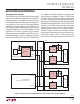
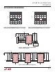
Interoperability is improved by reducing the interaction time
between the LTC4313 buffers and other RTAs by reducing
R1 and C
B1
. The following guidelines are recommended
for single supply systems,
a. For 5V systems choose R1 < 20kΩ and C
B1
< 1nF. There
are no other constraints.
b. For 3.3V systems, refer to Figures 11 and 12 for opera-
tion with LTC4300As and LTC4307s. In the figures,
M =
Number of LTC4300As or LTC4307s
Number of LTC4313s
R1 and C
B1
must be chosen to be below the curves
for a specific value of M. For M greater than the val-
ues shown in the figures, non-idealities do not result.
R1 <20kΩ and C
B1
<1nF are still recommended.
The LTC4313 is interoperable with non-compliant I
2
C
devices that drive a high V
OL
> 0.4V. Figure 13 shows the
LTC4313-1 in an application where a microcontroller com-
municates through the LTC4313-1 with a non-compliant
I
2
C device that drives a V
OL
of 0.6V. The LTC4313 buffers
are active up to a bus voltage of 0.3•V
CC
which is 1.089V
in this case, yielding a noise margin of 0.489V.
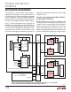
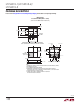
Repeater Application
Multiple LTC4313s can be cascaded in a repeater applica-
tion where a large 2-wire system is broken into smaller
sections as shown in Figure 14. The high noise margin
and low offset of the LTC4313 allows multiple devices
to be cascaded while still providing good system level
noise margin. In the repeater circuit shown in Figure 14 if
SCL1/SDA1 is driven externally to 200mV, SCL2/SDA2
is regulated to ~440mV worst-case by the cascade of
LTC4313-1s. The buffer turn-off voltage is 1.089V, yield-
ing a minimum logic low noise margin of ~650mV. In
Figure 14, use of the RTAs combined with an increased
level of buffering reduces transition times and permits
operation at a higher frequency.