
Datasheet

LTC4313-1/LTC4313-2/
LTC4313-3
5
4313123f
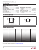
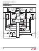
pin FuncTions
ENABLE (Pin 1): Connection Enable Input. When driven
low, the ENABLE pin isolates SDAIN and SCLIN from
SDAOUT and SCLOUT, asserts READY low, disables
rise time accelerators and inhibits automatic clock and
stop bit generation during a stuck low fault condition.
When driven high, the ENABLE pin connects SDAIN and
SCLIN to SDAOUT and SCLOUT after a stop bit or bus idle
has been detected on both busses. Driving ENABLE high
also enables automatic clock generation during a stuck
low fault condition. During a stuck low fault condition, a
rising edge on the ENABLE pin forces a connection between
SDAIN and SDAOUT and SCLIN and SCLOUT. When using
the LTC4313 in a Hot Swap™ application with staggered
connector pins, connect a 10k resistor between ENABLE
and GND to ensure correct functionality. Connect to V
CC
if unused.
SCLOUT (Pin 2): Serial Bus 2 Clock Input/Output. Connect
this pin to the SCL bus segment where stuck low recovery
is desired. Connect an external pull-up resistor or current
source between this pin and the bus supply. The bus supply
needs to be ≥ V
CC
for the LTC4313-1 and LTC4313-2, but
not for the LTC4313-3. Refer to the Applications Informa-
tion section for more details. Do not leave open.
SCLIN (Pin 3): Serial Bus 1 Clock Input/Output. Connect
this pin to the SCL line on the upstream bus. Connect
an external pull-up resistor or current source between
this pin and the bus supply. The bus supply needs to be
≥ V
CC
for the LTC4313-1 and LTC4313-2, but not for the
LTC4313-3. Refer to the Applications Information section
for more details. Do not leave open.
GND (Pin 4): Device Ground.
READY (Pin 5): Connection Ready Status Output. This
open drain N-channel MOSFET output pulls low when
the input and output sides are disconnected. READY is
pulled high when ENABLE is high and a connection has
been established between the input and output. Connect
a pull-up resistor, typically 10k from this pin to the bus
pull-up supply. Leave open or tie to GND if unused.
SDAIN (Pin 6): Serial Bus 1 Data Input/Output. Connect
this pin to the SDA line on the upstream bus. Connect an
external pull-up resistor or current source between this pin
and the bus supply. The bus supply needs to be ≥ V
CC
for
the LTC4313-1 and LTC4313-2, but not for the LTC4313-3.
Refer to the Applications Information section for more
details. Do not leave open.
SDAOUT (Pin 7): Serial Bus 2 Data Input/Output. Connect
this pin to the SDA bus segment where stuck low recovery
is desired. Connect an external pull-up resistor or current
source between this pin and the bus supply. The bus supply
needs to be ≥ V
CC
for the LTC4313-1 and LTC4313-2, but
not for the LTC4313-3. Refer to the Applications Informa-
tion section for more details. Do not leave open.
V
CC
(Pin 8): Power Supply Voltage. Power this pin from
a supply between 2.9V and 5.5V. Bypass with at least
0.01µF to GND.
Exposed Pad (Pin 9, DD8 Package Only): Exposed pad
may be left open or connected to device GND.