
Datasheet

LTC4313-1/LTC4313-2/
LTC4313-3
9
4313123f
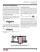
of the LTC4313-1 and LTC4313-2 must be greater than
or equal to 0.9•V
CC
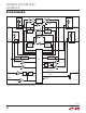
. An example is shown in Figure 3
where the input bus voltage is greater than V
CC
. During a
rising edge, the input bus rise rate will be accelerated by
the RTA up to a voltage of 2.97V after which the bus rise
rate will reduce to a value that is determined by the bus
current and bus capacitance. The RTA turn-off voltage is
less than the bus supply and the bus is not overdriven.
Pull-Up Resistor Value Selection
To guarantee that the RTAs are activated during a rising
edge, the bus must rise on its own with a positive slew rate
of at least 0.4V/µs. To achieve this, choose a maximum
R
BUS
using the formula:
R
BUS
≤
V
DD,BUS(MIN)
− V
RTA(TH)
( )
0.4
V
µs
• C
BUS
(1)
R
BUS
is the pull-up resistor, V
DD,BUS(MIN)
is the minimum
bus pull-up supply voltage, V
RTA(TH)
is the voltage at which
the RTA turns on and C
BUS
is the equivalent bus capaci-
tance. R
BUS
must also be large enough to guarantee that:
R
BUS
≥
V
DD,BUS(MAX)
− 0.4V
( )
4mA
(2)
This criterion ensures that the maximum bus current is
less than 4mA.
applicaTions inForMaTion
Input to Output Offset Voltage
While propagating a logic low voltage on its SDA and SCL
pins, the LTC4313 introduces a positive offset voltage
between the input and output. When a logic low voltage
≥200mV is driven on any of the LTC4313’s clock or data
pins, the LTC4313 regulates the voltage on the opposite
side to a slightly higher value. This is illustrated in Equa-
tion 3, which uses SDA as an example:
V
SDAOUT
= V
SDAIN
+ 50mV + 15Ω •
V
DD,BUS
R
BUS
(3)
In Equation 3, V
DD,BUS
is the output bus supply voltage
and R
BUS
is the SDAOUT bus pull-up resistance.
For driven logic low voltages < 200mV Equation 3 does
not apply as the saturation voltage of the open collector
output transistor results in a higher offset. For a driven input
logic low voltage below 220mV, the output is guaranteed
to be below a V
OL
of 400mV for bus pull-up currents up to
4mA. See the Typical Performance Characteristics section
for offset variation as a function of the driven logic low
voltage and bus pull-up current.
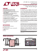
Figure 3. Level Shift Application Where the SDAIN and SCLIN Bus Pull-Up
Supply Voltage Is Higher Than the Supply Voltage of the LTC4313
LTC4313-1
GND
V
CC
4313123 F03
READY
SCLOUT
SDAOUT
ENABLE
SCLIN
SDAIN
SCL1
SDA1
R2
10k
C1
0.01µF
R1
10k
5V
READY
SCL2
SDA2
R4
10k
R3
10k
3.3V
R5
10k