
Datasheet
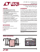

LTC4313-1/LTC4313-2/
LTC4313-3
7
4313123f
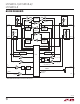
operaTion
The LTC4313 is a high noise margin bus buffer which
provides capacitance buffering for I
2
C signals. Capacitance
buffering is achieved by using back to back buffers on
the clock and data channels which isolate the SDAIN
and SCLIN capacitances from the SDAOUT and SCLOUT
capacitances respectively. All SDA and SCL pins are fully
bidirectional. The high noise margin allows the LTC4313 to
operate with non-compliant I
2
C devices that drive a high
V
OL
, permits a number of LTC4313s to be connected in
series and improves the reliability of I
2
C communications
in large noisy systems. Rise time accelerator (RTA) pull-up
currents (I
RTA
) turn on during rising edges to reduce bus
rise time for the LTC4313-1 and LTC4313-2. In a typical
application the input and output busses are pulled up to
V
CC
although this is not a requirement. If V
DD,BUS
is not
tied to V
CC
, V
DD,BUS
must be greater than V
CC
to prevent
overdrive of the bus by the RTAs for the LTC4313-1 and
LTC4313-2. See the Applications Information section for
V
DD,BUS
requirements for the LTC4313-3.
When the LTC4313 first receives power on its V
CC
pin, it
starts out in an undervoltage lockout mode (UVLO) until
its V
CC
exceeds 2.7V. The buffers and RTAs are disabled
and the LTC4313 ignores the logic state of its clock and
data pins. During this time the precharge circuit forces a
nominal voltage of 1V on the SDA and SCL pins through
200k resistors.
Once the LTC4313 exits UVLO and its ENABLE pin has
been asserted high, it monitors the clock and data pins
for a stop bit or a bus idle condition. When a combination
of either condition is detected simultaneously on the input
and output sides, the LTC4313 activates the connection
between SDAIN and SDAOUT, and SCLIN and SCLOUT,
respectively, asserts READY high and deactivates the
precharge circuit. RTAs for the LTC4313-1 and LTC4313-2
are also enabled at this time.
When a SDA/SCL pin is driven below the V
IL
level, the
buffers are turned on and the logic low level is propagated
though the LTC4313 to the other side. A high occurs when
all devices on the input and output sides release high. Once
the bus voltages rise above the V
IL
level, the buffers are
turned off. The RTAs are turned on at a slightly higher volt-
age. The RTAs accelerate the rising edges of the SDA/SCL
inputs and outputs up to a voltage of 0.9•V
CC
, provided
that the busses on their own are rising at a minimum rate
of 0.4V/µs as determined by the slew rate detectors. The
RTAs are configured to operate in a strong slew limited
switch mode in the LTC4313-1 and in the current source
mode in the LTC4313-2.
The LTC4313 detects a bus stuck low (fault) condition
when both clock and data busses are not simultaneously
high at least once in 45ms. When a stuck bus occurs, the
LTC4313 disconnects the input and output sides and after
waiting at least 40µs, generates up to sixteen 5.5kHz clock
pulses on the SCLOUT pin and a stop bit to attempt to free
the stuck bus. Should the stuck bus release high during
this period, automatic clock generation is terminated.
Once the stuck bus recovers, connection is re-established
between the input and output after a stop bit or bus idle
condition is detected. Toggling ENABLE after a fault condi-
tion has occurred forces a connection between the input
and output. When powering into a stuck low condition, the
input and output sides remain disconnected even after the
LTC4313 has exited the UVLO mode as a stop bit or bus
idle condition is not detected on the stuck busses. After
the timeout period, a stuck low fault condition is detected
and the behavior is as described previously.