
Datasheet

LTC4313-1/LTC4313-2/
LTC4313-3
8
4313123f
The LTC4313 provides capacitance buffering, data and
clock Hot Swap capability and level translation. The high
noise margin of the LTC4313 permits interoperability with
I
2
C devices that drive a high V
OL
permits series connec-
tion of multiple LTC4313s and improves I
2
C communica-
tion reliability. The LTC4313 isolates backplane and card
capacitances and provides slew control of falling edges
while level translating 3.3V and 5V busses. The LTC4313-1
and LTC4313-2 also provide pull-up currents to accelerate
rising edges. These features are illustrated in the following
subsections.
Rise Time Accelerator (RTA) Pull-Up Current Strength
(LTC4313-1 and LTC4313-2)
After an input and output connection has been established,
the RTAs on both the input and output sides of the SDA
and SCL busses are activated. During positive bus transi-
tions of at least 0.4V/µs, the RTAs provide pull-up cur-
rents to reduce rise time. The RTAs allow users to choose
larger bus pull-up resistors to reduce power consumption
and improve logic low noise margins, design with bus
capacitances outside of the I
2
C specification or to oper-
ate at a higher clock frequency. The LTC4313-1 regulates
its RTA current to limit the bus rise rate to a maximum
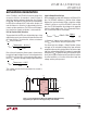
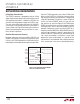
applicaTions inForMaTion
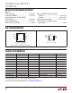
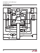
Figure 1. Bus Rising Edge for the LTC4313-1. V
CC
= V
DD,BUS
= 5V Figure 2. Bus Rising Edge for the LTC4313-2. V
CC
= V
DD,BUS
= 5V
of 75V/µs. The current is therefore directly proportional
to the bus capacitance. The LTC4313-1 RTA is capable of
sourcing up to 40mA of current. Rise time acceleration
for the LTC4313-2 is provided by a 2.5mA current source.
Figures 1 and 2 show the rising waveforms of heavily
loaded SDAIN and SDAOUT busses for the LTC4313-1 and
LTC4313-2 respectively. In both figures, during a rising
edge, the buffers are active and the input and output sides
are connected, until the bus voltages on both the input
and output sides are greater than 0.3 • V
CC
. When each
individual bus voltage rises above 0.41 • V
CC
, the RTA on
that bus turns on. The effect of the acceleration strength
is shown in the waveforms in Figures 1 and 2 for identi-
cal bus loads. The RTAs of the LTC4313-1 and LTC4313-2
supply 10mA and 2.5mA of pull-up current respectively for
the bus conditions shown in Figures 1 and 2. For identical
bus loads, the bus rises faster in Figure 1 compared to
Figure 2 because of the higher I
RTA
.
The RTAs are internally disabled during power-up and dur-
ing a bus stuck low event. The RTAs when activated pull
the bus up to 0.9•V
CC
on the input and output sides of the
SDA and SCL pins. In order to prevent bus overdrive by
the RTA, the bus supplies on the input and output sides
2V/DIV
1µs/DIV
4313123 F01
V
CC
= V
DD,BUS
= 5V
R
BUS
= 20k
C
IN
= C
OUT
= 200pF
SDAIN
SDAOUT
2V/DIV
1µs/DIV
4313123 F02
V
CC
= V
DD,BUS
= 5V
R
BUS
= 20k
C
IN
= C
OUT
= 200pF
SDAIN
SDAOUT