
Datasheet

LTC4314
11
4314f
R
BUS
values on each output channel must also be chosen
to ensure that when all the required output channels are
enabled, the total bus current is ≤4mA. The bus current
in each output channel can be 4mA if only one channel is
enabled at any given time. The R
BUS
value on the input must
also be chosen to limit the bus current to be ≤4mA. The
bus current for a single bus is determined by equation 2:
I
BUS
(A)=
V
DD,BUS
− 0.4V
R
BUS
(2)
Input to Output Offset Voltage and Propagation Delay
The LTC4314 introduces both an offset as well as a
propagation delay for falling edges between the input
and output. When a logic low voltage ≥ 200mV is driven
on any of the LTC4314’s data or clock pins, the LTC4314
regulates the voltage on the opposite side to a slightly
higher value. When SCLIN or SDAIN is driven to a logic
low voltage, SCLOUT or SDAOUT is driven to a slightly
higher voltage, as directed by equation 3 which uses SDA
as an example:
V
SDAOUT
(V)= V
SDAIN
+ 45mV
+ (10Ω + R
MUX
)•
V
DD,BUS
R
BUS
(3)
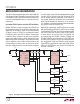
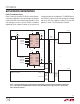
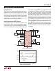
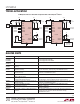
Figure 4. Connection of the LTC4314 in a Level Shift Application. V
CC
is Less than or Equal to the Minimum
Bus Supply Voltages on the Output Side. V
CC2
is Grounded to Disable Output Rise Time Accelerators
LTC4314
GND
V
CC
V
CC2
4314 F04
SCLOUT1
SDAOUT1
SCLOUT4
SDAOUT4
SCLOUT1
SDAOUT1
SCLOUT4
SDAOUT4
SCLIN
SDAIN
ENABLE1
ENABLE2
ENABLE3
ENABLE4
ACC
DISCEN
FAULT
SCLIN
SDAIN
ENABLE1
ENABLE2
ENABLE3
ENABLE4
3.3V
FAULT
R3
10k
R2
10k
R1
10k
C1
0.01μF
C2
0.01μF
3.3V 3.3V
R5
10k
R4
10k
5V
R7
10k
R6
10k
•••
•••
APPLICATIONS INFORMATION
V
DD, BUS
is the output bus voltage, R
BUS
is the output bus
pull-up resistance and R
MUX
is the resistance of the channel
transmission gate in the multiplexer shown in the block
diagram. The offset is affected by the V
CC2
voltage and bus
current. A higher V
CC2
voltage (V
CC
if V
CC2
is grounded)
reduces R
MUX
leading to a lower offset. See the Typical
Performance Characteristics plots for the variation of R
MUX
as a function of V
CC2
and temperature. When SCLOUT or
SDAOUT is driven to a logic low voltage ≥ 200mV, SCLIN
or SDAIN is regulated to a logic low voltage, as directed
by equation 4 which uses SDA as an example:
V
SDAIN
(V)= V
SDAOUT
+ 45mV +10Ω •
V
DD, BUS
R
BUS
(4)
The SCLOUT/SDAOUT to SCLIN/SDAIN offset is lower than
the reverse case as the multiplexer transmission gate does
not affect this offset. For driven logic low voltages <200mV,
the above equations do not apply as the saturation voltage
of the open collector output transistor results in a higher
offset. However, the offset is guaranteed to be less than
400mV for a total bus pull-up current of 4mA under all
conditions. See the Typical Performance Characteristics
curves for the buffer offset voltages as a function of the
driven logic low voltage and bus pull-up current.