
Datasheet

LTC4314
12
4314f
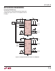
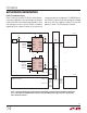
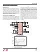
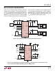
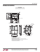
Figure 5. Cascading an LTC4314 with Another LTC4314 and LTC Bus Buffers. Only the SCL Pathway Is Shown for Simplicity
APPLICATIONS INFORMATION
The high-to-low propagation delay arises due to both the
fi nite response time of the buffers and their fi nite current
sink capability. See the Typical Performance Characteristics
curves for the propagation delay as a function of the bus
capacitance.
Cascading LTC4314 devices and other LTC Bus Buffers
Multiple LTC4314s can be cascaded or the LTC4314 can
be cascaded with other LTC bus buffers as required by the
application. An example is shown for the clock pathway
in Figure 5 where an LTC4314 is cascaded with another
LTC4314 and some select LTC bus buffers. The data path
is identical. When using such cascades, users should be
aware of the additive logic low offset voltages V
OS
when
determining system noise margin. If the sum of the offsets
(refer to equations 3 and 4 and to the data sheets of the
corresponding bus buffers) plus the worst-case driven
logic low voltage across the cascade exceeds the buffer
turn-off voltage, signals will not be propagated across the
cascade. Also the minimum rise time accelerator (RTA)
turn-on voltage (wherever applicable) of each device in
the cascade should also be greater than the maximum
buffer turn-off voltage of all the devices in the cascade.
This condition is required to prevent contention between
one device’s buffer and another’s RTA.
Based on this requirement, the LTC4314 can be cascaded
with the LTC4303 and LTC4307 if its RTA turn-on voltage
is set to be 0.8V (ACC low). The LTC4314 can be cascaded
with the LTC4301 and LTC4301L under all ACC settings
as these devices do not have RTAs. The LTC4314 can
be cascaded with the LTC4302, LTC4304, LTC4305 and
LTC4306 if its RTAs are set to turn on at 0.8V (ACC low)
or under all ACC settings if the RTAs on the other bus buf-
fers are disabled. Finally two LTC4314s can be cascaded
if their ACC pins are tied to the same state, HIGH, LOW or
OPEN, or if the ACC pin of one LTC4314 is tied high and
the other is left open.
LTC4314
GND
V
CC
V
CC2
4314 F05
SCLOUT1
SCLOUT2
SCLOUT3
SCLOUT4
SCLIN
ACC
SCLIN
R1
10k
C1
0.01μF
3.3V
R3
10k
R2
10k
5V
R5
10k
R4
10k
LTC4314
GND
V
CC
V
CC2
SCLOUT1
SCLOUT4
SCLIN
ACC
LTC4301
GND
V
CC
SCLOUTSCLIN
SCLOUT1
SCLOUT4
SCLOUT5
3.3V
3.3V
R6
10k
R7
10k
LTC4303
GND
V
CC
SCLOUTSCLIN
SCLOUT6
5V
R8
10k
LTC4307
GND
V
CC
SCLOUTSCLIN
SCLOUT7
5V
R9
10k
C2
0.01μF
ttt
ttt