
Datasheet

LTC4314
16
4314f
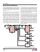
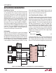
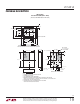
Figure 10. The LTC4314 Confi gured as a 2:1 Demultiplexer in a System with Redundancy
LTC4314
GND
V
CC2
V
CC
4314 F10
SDAIN
SCLIN
ACC
DISCEN
FAULT
SDAOUT1
SCLOUT1
ENABLE1
SDAOUT2
SCLOUT2
ENABLE2
SDAOUT3
SCLOUT3
ENABLE3
SDAOUT4
SCLOUT4
ENABLE4
C1
0.01μF
SDA
SCL
FAULT
3.3V
R9
10k
R8
10k
R1
10k
R2
10k
5V
R3
10k
R4
10k
R5
100k
3.3V
R10
10k
R7
20k
BFP405F
R6
50k
PRIMARY
I
2
C
MASTER
CONTROLLER
CARD
BACKUP
I
2
C
MASTER
CONTROLLER
CARD
APPLICATIONS INFORMATION
Demultiplexer Function
Due to its bi-directional nature, the LTC4314 can be used
as a demultiplexer. This is shown in Figure 10 where two
channels are used to drive I
2
C data from the master side
with redundancy to the slave side. In this application the
SDAOUT/SCLOUT channels serve as the inputs while the
SDAIN/SCLIN channel is the output. Redundancy on the
master side provides protection against power supply
failure. In Figure 10, if the 5V bus supply on channel 1
falls below 1.4V, channel 1 gets disabled as ENABLE1 is
driven below its digital threshold. Simultaneously, the V
BE
of the pull-down device on ENABLE4 falls below 0.7V and
it turns off. This causes ENABLE4 to be pulled up by R7
which in turn enables channel 4, causing control to be
transferred to the backup I
2
C master device.
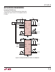
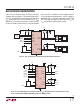
Hot-Swapping
Figure 11 shows the LTC4314 in a typical hot-swapping
application where the LTC4314 is on the backplane and I/O
cards plug into the downstream channels. The outputs must
idle high and the corresponding output channel must be
disabled before an I/O card can be plugged or unplugged
from an output channel. Figure 11 also shows the use of
a non-compliant I
2
C device with the LTC4314. The high
noise margin of the LTC4314 supports logic low levels up
to 0.3 • V
CC
, allowing devices to drive greater than 0.4V
logic low levels on the block and data lines.
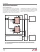
Level Translating to Bus Voltages < 2.25V
The LTC4314 can be used for level translation to bus volt-
ages below 2.25V if certain conditions are met. In order to
perform this level translation, RTAs on the low voltage side
need to be disabled in order to prevent an over drive of
the low voltage bus. This can be accomplished by forcing
ACC high or grounding V
CC2
. If one of the output chan-
nels is pulled up to the low voltage bus supply, all other
output channels need to be disabled when this channel
is active, in order to prevent cross conduction between
the output channels. Since the buffer turn-on and turn-off
voltages are 0.3•V
MIN
, the minimum bus supply voltage
is determined by equation 5:
V
DD,BUS(MIN)
≥
0.3 • V
MIN
0.7
(5)
in order to meet the V
IH
= 0.7 •V
DD,BUS
requirement and
not impact the high side noise margin. Users willing to live
with a lower logic high noise margin can level translate
down to 1.5V. An example of voltage level translation from