
Datasheet
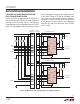
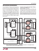
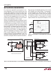
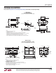
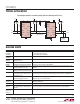
Table Of Contents

LTC4315
13
4315f
APPLICATIONS INFORMATION
In Figure 6, a staggered connector is used to connect the
LTC4315 to the backplane. V
CC
and GND are the longest
pins to ensure that the LTC4315 is powered and forcing
a 1V precharge voltage on the medium length SDA and
SCL pins before they contact the backplane. The 1V pre-
charge voltage is applied to the SDA and SCL pins through
200k resistors. Since cards are being plugged into a live
backplane whose SDA and SCL busses could be at any
voltage between 0 and V
CC
, precharging the LTC4315’s
SDA and SCL pins to 1V minimizes disturbances to the
backplane bus when cards are being plugged in. The low
(<10pF) input capacitance of the LTC4315 also contributes
to minimizing bus disturbance as cards are being plugged
in. With ENABLE being the shortest pin and also pulled to
GND by a resistor, the staggered approach provides ad-
ditional time for transients associated with live insertion to
settle before the LTC4315 can be enabled. A 10k or lower
pull-down resistor from ENABLE to GND is recommended.
If a connector is used where all pins are of equal length,
the benefit of the precharge circuit is lost. Also, the
ENABLE signal to the LTC4315 must be held low until all
transients associated with the plugging in of a card into
a live system die out.
LEVEL TRANSLATING TO VOLTAGES <2.25V
The LTC4315 can be used for level translation to bus volt-
ages below 2.25V if certain conditions are met. In order
to perform this level translation, RTAs on the low voltage
side need to be disabled in order to prevent an overdrive
of the low voltage bus. Since the maximum buffer turn-on
and turn-off voltages are 0.36 • V
MIN
, the minimum bus
supply voltage is determined by the following equation,
V
DD,BUS(MIN)
≥
0.36 • V
MIN
0.7
(4)
in order to meet the V
IH
= 0.7 • V
DD,BUS
requirement and
not impact the logic high noise margin. Voltage level
translation down to 1.4V is allowed, but the logic high
noise margin will be lowered. An example of voltage level
translation from 3.3V to 1.8V is illustrated in Figure 7,
where a 3.3V input voltage bus is translated to a 1.8V
output voltage bus. Tying V
CC
to 3.3V satisfies Equation 4.
Grounding V
CC2
disables the output RTAs. V
MIN
defaults
to V
CC
under these conditions, making the buffer turn-off
voltage 1.089V. A similar voltage translation can also be
performed going from a 3.3V bus supply on the output
side to a 1.8V bus supply on the input side if ACC is tied
high to disable the input RTAs and if V
CC
and V
CC2
are
tied to the 3.3V bus supply.
Figure 7. Voltage Level Translation from 3.3V to 1.8V Using
the LTC4315
LTC4315
GND
V
CC
V
CC2
4315 F07
SCLOUT
SDAOUT
FAULT
DISCEN
ENABLE
SCLIN
SDAIN
ACC
SCL1
SDA1
R2
10k
R5
10k
R6
10k
R4
10k
R3
10k
R1
10k
3.3V
READY
SCL2
SDA2
FAULT
1.8V
C1
0.01µF
READY