
Datasheet
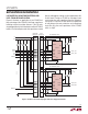

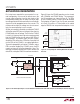
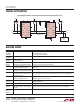
Table Of Contents

LTC4315
11
4315f
APPLICATIONS INFORMATION
INPUT TO OUTPUT OFFSET VOLTAGE
While propagating a logic low voltage on its SDA and SCL
pins, the LTC4315 introduces a positive offset voltage
between the input and output. When a logic low voltage
≥200mV is driven on any of the LTC4315’s data or clock
pins, the LTC4315 regulates the voltage on the oppo-
site side to a slightly higher value. This is illustrated in
Equation 3, which uses SDA as an example:
V
SDAOUT
= V
SDAIN
+ 50mV + 15Ω •
V
DD,BUS
R
BUS
(3)
In Equation 3, V
DD,BUS
is the output bus supply voltage
and R
BUS
is the SDAOUT bus pull-up resistance.
For driven logic low voltages < 200mV Equation 3 does
not apply as the saturation voltage of the open collector
output transistor results in a higher offset. However, for
any input logic low below 220mV, the output is guaranteed
to be below a V
OL
of 400mV for bus pull-up currents up
to 4mA. See the Typical Performance section for offset
variation as a function of the driven logic low voltage and
bus pull-up current.
FALLING EDGE CHARACTERISTICS
The LTC4315 introduces a propagation delay on falling
edges due to the finite response time and finite current
sink capability of its buffers. In addition the LTC4315 also
slew limits the falling edge to an edge rate of 45V/µs.
The slew limited falling edge eliminates fast transitions
on the busses and minimizes transmission line effects
in systems. Refer to the Typical Performance section for
the propagation delay and fall times as a function of the
bus capacitance.
STUCK BUS DISCONNECT AND RECOVERY
During an output bus stuck low condition (SCLOUT or
SDAOUT stuck low for at least 45ms) if DISCEN is tied
high, the LTC4315 attempts to unstick the bus by first
breaking the connection between the input and output. The
LTC4315 then asserts FAUL T low and after 40µs, gener-
ates up to sixteen 5.5KHz clock pulses on the SCLOUT
pin. Should the stuck bus release high during this period,
clock generation is stopped, a stop bit is generated and the
FAUL T flag is cleared. This process is shown in Figure 5
for the case where SDAOUT starts out stuck low and then
recovers. As seen from the figure, the LTC4315 pulls FAUL T
and READY low and breaks the connection between the
input and output sides, when a stuck low condition on
SDA is detected. Clock pulses are then issued on SCLOUT
to attempt to unstick the SDAOUT bus. When SDAOUT
recovers, clock pulsing is stopped, a stop bit is generated
on the output and FAUL T and READY are released high. If
DISCEN is low and a stuck bus event occurs, the FAUL T
flag is driven low but the input and output sides stay con-
n e c t e d a n d n o c l o c k i n g o r s t o p b i t g e n e r a t i o n o c c u r s . W h e n
powering up into a stuck low condition, a connection is
never made between the input and the output, as a stop
bit or bus idle condition is never detected. After a timeout
period of 45ms, the FAUL T flag is asserted low and the
behavior is the same as described previously.
Figure 5. Bus Waveforms During SDAOUT Stuck Low
and Recovery Event
4315 F05
FAULT
5V/DIV
SCLOUT
5V/DIV
READY
5V/DIV
SDAIN
5V/DIV
SDAOUT
5V/DIV
1ms/DIV
AUTOMATIC CLOCKING
DISCONNECT
AT TIMEOUT
STUCK LOW > 45ms
RECOVERS
HIGH
DRIVEN
LOW
STOP BIT
GENERATED