
Datasheet
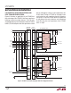
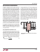

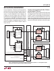
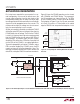
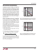
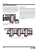
Table Of Contents

LTC4315
16
4315f
APPLICATIONS INFORMATION
First, when two or more buffers are connected in a cas-
cade configuration, if the sum of the offsets across the
cascade (refer to Equation 3 and the data sheets of the
corresponding buffers) plus the worst-case driven logic
low voltage exceeds the minimum buffer turn-off voltage,
signals will not be propagated across the cascade. The
maximum driven logic low voltage must be set accord-
ingly, for correct operation in such cascades.
Second, noise margin is affected by cascading the LTC4315
with buffers whose RTA turn-on voltage is lower than the
LTC4315 buffer turn-off voltage. The V
IL
for the LTC4315
is set to 0.3 • V
MIN
to achieve high noise margin provided
that the LTC4315 buffers do not contend with RTAs of
other products. To maximize logic low noise margin,
disable the RTAs of the other LTC buffers if possible and
use the RTAs of the LTC4315 in cascading applications.
To permit interoperability with other LTC buffers whose
RTAs cannot be disabled, the LTC4315 senses the RTA
current and turns off its buffers below 0.3 • V
MIN
. This
eliminates contention between the LTC4315 buffers and
other RTAs, making the SDA/SCL waveforms monotonic.
Figure 10. The LTC4315 Operating in a Cascade with Other LTC Buffers with Active RTAs. Only the Clock Pathway Is Shown for Simplicity
Figure 11. Corresponding SCL Switching Waveforms. No Glitches
Are Seen.
Figure 10 shows the LTC4315 operating on a bus shared
with LTC4300A and LTC4307 buffers. The correspond-
ing SCL waveforms are shown in Figure 11. The RTAs
on the LTC4300A and the LTC4307 cannot be disabled.
The backplane in Figure 11 has five I/O cards connected
to it. Each I/O card has a LTC bus buffer on its outside
edge for SDA/SCL hot swap onto the backplane. In this
4315 F10
LTC4315
GND
V
CC
V
CC2
SCLOUTSCLIN
ACC
SCL1
R3
2.7k
R1
5k
C1
0.01µF
3.3V
I/O CARD #1 I/O CARD #2 TO #4
I/O CARD #5
CB1
100pF
*CB2
690pF
*PARASITIC BACKPLANE CAPACITANCE
R2
2.7k
5V
SCL2
BACKPLANE
R4
5k
LTC4300A
GND
V
CC
SCLOUTSCLIN SCL3
LTC4307
GND
V
CC
SCLOUTSCLIN
SCL4
1µs/DIV
SCL3
2V/DIV
SCL2
2V/DIV
SCL1
2V/DIV
4315 F11
LTC4315
RTA
TURNS ON
LTC4300A/
LTC4307
RTAs
TURN ON
LTC4315
BUFFERS
TURN OFF