
Datasheet
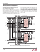
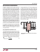

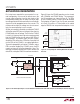
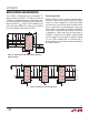
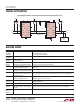
Table Of Contents

LTC4315
18
4315f
APPLICATIONS INFORMATION
The LTC4315 is interoperable with non-compliant I
2
C
devices that drive a high V
OL
> 0.4V. Figure 14 shows the
LTC4315 in an application where a microcontroller com-
municates through the LTC4315 with a non-compliant I
2
C
device that drives a V
OL
of 0.6V. The LTC4313 buffers are
active up to a bus voltage of 0.3 • V
MIN
which is 1.089V in
this case, yielding a noise margin of 0.489V.
Figure 15. LTC4315s in a Repeater Application
LTC4315
GND
V
CC
V
CC2
4315 F15
READY
SCLOUT
SDAOUT
FAULT
DISCEN
ENABLE
SCLIN
SDAIN
ACC
SCL1
SDA1
R2
10k
R3
10k
R4
10k
R1
10k
C1
0.01µF
3.3V
LTC4315
GND
V
CC
V
CC2
READY
SCLOUT
SDAOUT
FAULT
DISCEN
ENABLE
SCLIN
SDAIN
ACC
R6
10k
R5
10k
LTC4315
GND
V
CC
V
CC2
READY
SCLOUT
SDAOUT
FAULT
DISCEN
ENABLE
SCLIN
SDAIN
ACC
R9
10k
R10
10k
R8
10k
R7
10k
SCL2
SDA2
READY
FAULT
Repeater Application
Multiple LTC4315s can be cascaded in a repeater applica-
tion where a large 2-wire system is broken into smaller
sections as shown in Figure 15. The high noise margin
and low offset of the LTC4315 allows multiple devices
to be cascaded while still providing good system level
noise margin. In the repeater circuit shown in Figure 15,
if SCL1/SDA1 is driven externally to 200mV, SCL2/SDA2
is regulated to ~440mV worst-case by the cascade of
LTC4315s. The buffer turn-off voltage is 1.089V yielding
a minimum logic low noise margin of ~650mV. In Figure
15, use of RTAs combined with an increased level of
buffering reduces transition times and permits operation
at a higher frequency.
Figure 14. Communication with a Non-Compliant I
2
C Device
Using the LTC4315.
LTC4315
GND
V
CC
V
CC2
4315 F14
SCLOUT
SDAOUT
DISCEN
ENABLE
FAULT
READY
SCLIN
SDAIN
ACC
R6
10k
R3
10k
R4
10k
R2
10k
R1
10k
R5
10k
NON-COMPLIANT
I
2
C DEVICE
V
OL
= 0.6V
5V
3.3V
µP
C1
0.01µF