
Datasheet
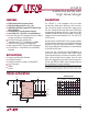

Table Of Contents
LTC4315
9
4315f
The LTC4315 provides capacitance buffering, data and
clock Hot Swap capability and level translation of I
2
C signals
on its clock and data pins. The high noise margin of the
LTC4315 permits interoperability with I
2
C devices that drive
a high V
OL
, permits series connection of multiple LTC4315s
and provides improved I
2
C communication reliability.
The LTC4315 isolates backplane and card capacitances,
provides slew limited acceleration of rising edges and slew
control of falling edges while level translating 1.5V, 1.8V,
2.5V, 3.3V and 5V busses. These features are illustrated
in the following subsections.
RISE TIME ACCELERATOR (RTA) PULL-UP CURRENT
STRENGTH
After an input to output connection has been established
the RTAs on both the input and output sides of the SDA
and SCL busses are activated based on the state of the
ACC pin and the V
CC2
supply voltage. During positive bus
transitions of at least 0.4V/µs, the RTAs provide pull-up
currents to reduce rise time. Enabling the RTAs allows
users to choose larger bus pull-up resistors to reduce
power consumption and improve logic low noise margins,
to design with bus capacitances outside of the I
2
C speci-
fication and to operate at a higher clock frequency. The
function of the ACC pin in setting I
RTA
is summarized in
Table 1. In the strong mode (ACC low) the acceleration is
slew limited to a maximum bus rise rate of 75V/µs. The
strong mode current is therefore directly proportional to
the bus capacitance. The LTC4315 is capable of sourcing
up to 40mA of current in the strong mode. If ACC is left
o p e n, r i s e t i m e a c c e l er a t i o n i s p r ov i d e d b y a 2. 5 m A p ul l u p.
TABLE 1: ACC Control of the RTA Current I
RTA
ACC I
RTA
Low Strong
Hi-Z 2.5mA
High None
The ACC pin has a resistive divider between V
CC
and ground
to set its voltage to 0.5 • V
CC
if left open.
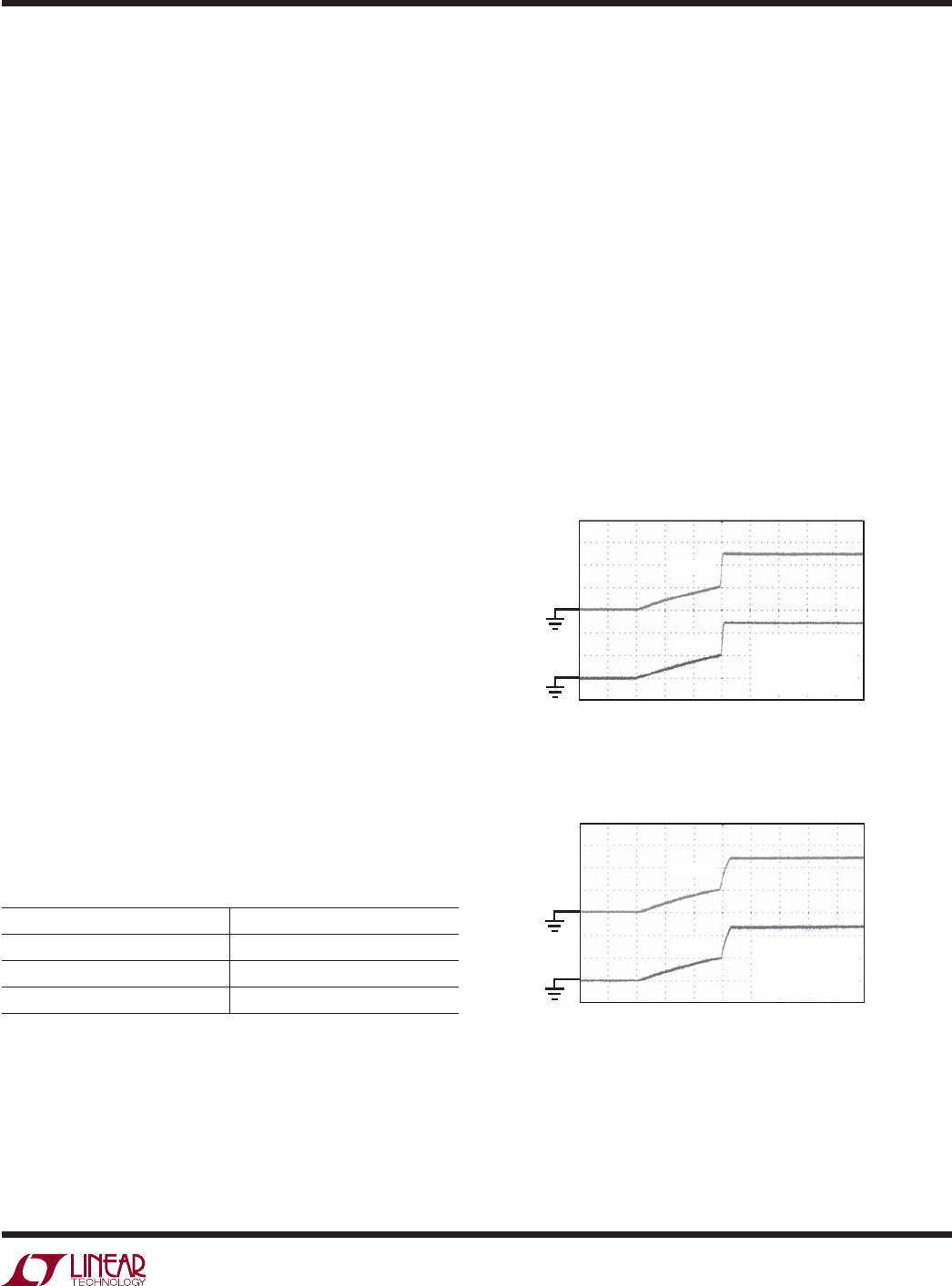
APPLICATIONS INFORMATION
Figures 1 and 2 show the rising waveforms of heavily
loaded SDAIN and SDAOUT busses with the ACC pin set for
strong mode and 2.5mA current source mode respectively.
In both figures, during a rising edge, the buffers are active
and the input and output sides connected, until the bus
voltages on both the input and output sides are greater than
0.33 • V
MIN
, where V
MIN
is the lower of the V
CC
and V
CC2
voltages. When each individual bus voltage rises above
0.41 • V
MIN
, the RTA on that bus turns on. The effect of the
acceleration strength is shown in the SDA waveforms in
Figures 1 and 2 for identical bus loads. The RTAs supply
10mA and 2.5mA of pull-up current I
RTA
in the strong and
current source modes respectively for the bus conditions
shown in Figures 1 and 2. For identical bus loads, the bus
rises faster in Figure 1 compared to Figure 2 because of
the higher I
RTA
.
Figure 1. Bus Rising Edge for the Strong Acceleration Mode.
V
CC
= V
CC2
= 5V
Figure 2. Bus Rising Edge for the Current Source
Acceleration Mode. V
CC
= V
CC2
= 5V
2V/DIV
1µs/DIV
4315 F01
V
CC
= V
CC2
= 5V
R
BUS
= 20k
C
IN
= C
OUT
= 200pF
ACC = 0V
SDAIN
SDAOUT
2V/DIV
1µs/DIV
4315 F02
V
CC
= V
CC2
= 5V
R
BUS
= 20k
C
IN
= C
OUT
= 200pF
ACC = OPEN
SDAIN
SDAOUT