
Datasheet


LTC4359
10
Rev. E
For more information www.analog.com
Figure10 shows a +48V application with reverse input
protection where D5 is used instead of R1 to eliminate
the power dissipation and system ground current when the
input reverses to –48V. With –48V input and OUT powered
by another supply or held up by output capacitance, D2
(5.1V) and D3 (75V) prevent the LTC4359’s OUT–IN pins
from exceeding the 100V absolute maximum rating. R2
limits the current into D1, D2 and D3 during a reverse input.
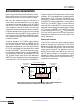
Paralleling Supplies
Multiple LTC4359s can be used to combine the outputs of
two or more supplies for redundancy or for droop sharing,
as shown in Figure5. For redundant supplies, the supply
with the highest output voltage sources most or all of the
load current. If this supply’s output is quickly shorted to
ground while delivering load current, the flow of current
temporarily reverses and flows backwards through the
LTC4359’s MOSFET. The LTC4359 senses this reverse
current and activates a fast pull-down to quickly turn off
the MOSFET.
APPLICATIONS INFORMATION
LTC4359
V
SS
IN
D2A
SMAJ24CA
24V
OUT
C
OUTA
1.5µF
C
OUTB
1.5µF
GATE
Q1A
FDMS86101
12V
10A
BUS
R1A
1k
LTC4359
V
SS
IN
SOURCE
SHDN
SOURCE OUTGATE
Q1B
FDMS86101
PSA
V
INA
= 12V
RTNA
PSB
V
INB
= 12V
RTNB
D2B
SMAJ24CA
24V
4359 F05
R1B
1k
SHDN
Figure5. Redundant Power Supplies
If the other, initially lower, supply was not delivering any
load current at the time of the fault, the output falls until
the body diode of its ORing MOSFET conducts. Meanwhile,
the LTC4359 charges the MOSFET gate with 10µA until
the forward drop is reduced to 30mV. If this supply was
sharing load current at the time of the fault, its associated
ORing MOSFET was already driven partially on. In this case,
the LTC4359 will simply drive the MOSFET gate harder in
an effort to maintain a drop of 30mV.
Droop sharing can be accomplished if both power supply
output voltages and output impedances are nearly equal.
The 30mV regulation technique ensures smooth load
sharing between outputs without oscillation. The degree
of sharing is a function of MOSFET R
DS(ON)
, the output
impedance of the supplies and their initial output voltages.
Load Switching and Inrush Control
By adding a second MOSFET as shown in Figure6, the
LTC4359 can be used to control power flow in the for-
ward direction while retaining ideal diode behavior in the
reverse direction. The body diodes of Q1 and Q2 prohibit
ON OFF
4359 F06
LTC4359
V
SS
IN OUT
SHDN
GATESOURCE
Q1
FDMS86101
R4
10k
C1
10nF
V
IN
28V
Q2
FQA140N10
R3
10Ω
V
OUT
28V
10A
C
LOAD
C
OUT
1.5µF
R1
1k
D4
DDZ9699T
12V
D1
SMAJ58A
58V
D2
SMAJ24A
24V
Figure6. 28V Load Switch and Ideal
Diode with Reverse Input Protection
Downloaded from Arrow.com.Downloaded from Arrow.com.Downloaded from Arrow.com.Downloaded from Arrow.com.Downloaded from Arrow.com.Downloaded from Arrow.com.Downloaded from Arrow.com.Downloaded from Arrow.com.Downloaded from Arrow.com.Downloaded from Arrow.com.