
Datasheet


LTC4359
11
Rev. E
For more information www.analog.com
APPLICATIONS INFORMATION
current flow when the MOSFETs are off. Q1 serves as the
ideal diode, while Q2 acts as a switch to control forward
power flow. On/off control is provided by the SHDN pin,
and C1 and R4 may be added if inrush control is desired.
When SHDN is driven high and provided V
IN
>V
OUT
+ 30mV,
GATE sources 10µA and gradually charges C1, pulling up
both MOSFET gates. Q2 operates as a source follower and
I
INRUSH
=
10µA • C
LOAD
C1
If V
IN
<V
OUT
+ 30mV, the LTC4359 will be activated but
holds Q1 and Q2 off until the input exceeds the output by
30mV. In this way normal diode behavior of the circuit is
preserved, but with soft starting when the diode turns on.
When SHDN is pulled low, GATE pulls the MOSFET gates
down quickly to SOURCE turning off both forward and
reverse paths, and the input current is reduced to 9µA.
While C1 and R4 may be omitted if soft starting is not
needed, R3 is necessary to prevent MOSFET parasitic
oscillations and must be placed close to Q2.
Layout Considerations
Connect the IN, SOURCE and OUT pins as close as possible
to the MOSFET source and drain pins. Keep the traces to
the MOSFET wide and short to minimize resistive losses as
shown in Figure 7. Place surge suppressors and necessary
transient protection components close to the LTC4359
using short lead lengths.
For the DFN package, pin spacing may be a concern at
voltages greater than 30V. Check creepage and clearance
guidelines to determine if this is an issue. To increase the
effective pin spacing between high voltage and ground pins,
leave the exposed pad connection open. Use no-clean flux
to minimize PCB contamination.
Figures 8 through 18 show typical applications of the
LTC4359.
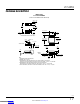
Figure 7a. Layout, DCB6 Package
Figure 7b. Layout, MS8/S8 Package
Figure8. 1.2V Diode–OR
4359 F07a
S
S
S
G
1
2
3
4
8
7
6
5
D
D
D
D
V
IN
OUT
LTC4359
GATE
IN
DCB6
4
5
7
6
3
2
1
V
OUT
SOURCE
MOSFET
LTC4359
S
S
S
G
1
2
3
4
8
7
6
5
D
D
D
D
MOSFET
GATE
IN
SOURCE
OUT
MS8/S8
4359 F07b
V
IN
V
OUT
LTC4359
V
SS
IN OUTGATE
Q1A
BSC011N03LS
–12V
–12V
V
OUT
1.2V
20A
R1A
1k
SOURCE
V
INA
1.2V
C
LOAD
C
OUTA
47nF
LTC4359
V
SS
IN OUTGATE
Q1B
BSC011N03LS
4359 F08
R1B
1k
SOURCE
V
INB
1.2V
C
OUTB
47nF
Downloaded from Arrow.com.Downloaded from Arrow.com.Downloaded from Arrow.com.Downloaded from Arrow.com.Downloaded from Arrow.com.Downloaded from Arrow.com.Downloaded from Arrow.com.Downloaded from Arrow.com.Downloaded from Arrow.com.Downloaded from Arrow.com.Downloaded from Arrow.com.