
Datasheet


LTC4359
8
Rev. E
For more information www.analog.com
APPLICATIONS INFORMATION
The MOSFET’s on-resistance, R
DS(ON)
, directly affects
the forward voltage drop and power dissipation. Desired
forward voltage drop should be less than that of a diode
for reduced power dissipation; 100mV is a good starting
point. Choose a MOSFET which has:
R
DS(ON)
<
Forward Voltage Drop
I
LOAD
The resulting power dissipation is
P
d
= (I
LOAD
)
2
• R
DS(ON)
Shutdown Mode
In shutdown, the LTC4359 pulls GATE low to SOURCE,
turning off the MOSFET and reducing its current consump
-
tion to 9µA. Shutdown does not interrupt forward current
flow, a path is still present through Q1’s body diode, as
shown in Figure1. A second MOSFET is needed to block
the forward path; see the section Load Switching and
Inrush Control. When enabled the LTC4359 operates as
an ideal diode. If shutdown is not needed, connect SHDN
to IN. SHDN may be driven with a 3.3V or 5V logic sig
-
nal, or with an open drain or collector. To assert SHDN
low
, the pull down must sink at least 5µA at 500mV. To
enable the part, SHDN must be pulled up to at least 2V.
If SHDN is driven with an open drain, open collector or
switch contact, an internal pull-up current of 2.6µA (1µA
minimum) asserts SHDN high and enables the LTC4359.
If leakage from SHDN to ground cannot be maintained at
less than 100nA, add a pull-up resistor to >2V to assure
turn on. The self-driven open circuit voltage is limited
internally to 2.5V. When floating, the impedance is high
and SHDN is subject to capacitive coupling from nearby
clock lines or traces exhibiting high dV/dt. Bypass SHDN
to V
SS
with 10nF to eliminate injection. Figure 3a is the
simplest way to control the shutdown pin. Since the control
signal ground is different from the SHDN pin reference,
V
SS
, there could be momentary glitches on SHDN during
transients. Figures 3b and 3c are alternative solutions
that level-shift the control signal and eliminate glitches.
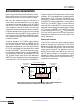
Figure 3a. SHDN Control
Figure 3b. Transistor SHDN Control
Figure 4c. Opto-Isolator SHDN Control
4359 F03a
LTC4359
R1
1k
Q4
VN2222LL
V
SS
SHDN
OFFON
4359 F03b
LTC4359
R1
1k
R7
240k
R5
100k
R6
100k
R8
240k
48V
Q4
2N5551
V
SS
SHDN
IN
ON
OFF
Q5
2N5401
4359 F03c
LTC4359
R1
1k
R5
2MΩ
R6
1MΩ
Q4
MOC
207M
R7
2k
48V
V
SS
SHDN
IN
OFFON
Input Short-Circuit Faults
The dynamic behavior of an active, ideal diode entering
reverse bias is most accurately characterized by a delay
followed by a period of reverse recovery. During the delay
phase some reverse current is built up, limited by parasitic
resistances and inductances. During the reverse recovery
Downloaded from Arrow.com.Downloaded from Arrow.com.Downloaded from Arrow.com.Downloaded from Arrow.com.Downloaded from Arrow.com.Downloaded from Arrow.com.Downloaded from Arrow.com.Downloaded from Arrow.com.