
Datasheet


LTC4359
9
Rev. E
For more information www.analog.com
phase, energy stored in the parasitic inductances is trans-
ferred to other elements in the circuit. Current slew rates
during reverse recovery may reach 100A/µs or higher.
High slew rates coupled with parasitic inductances in
series with the input and output paths may cause poten-
tially destructive transients to appear at the IN, SOURCE
and OUT pins of the LTC4359 during reverse recovery.
A zero impedance short-circuit directly across the input
and ground is especially troublesome because it permits
the highest possible reverse current to build up during
the delay phase. When the MOSFET finally interrupts the
reverse current, the LTC4359 IN and SOURCE pins experi-
ence a negative voltage spike, while the OUT pin spikes in
the positive direction.
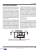
T
o prevent damage to the LTC4359 under conditions
of input short-circuit, protect the IN, SOURCE and OUT
pins as shown in Figure4. The IN and SOURCE pins are
protected by clamping to the V
SS
pin with two TransZorbs
or TVS. For input voltages 24V and greater, D4 is needed
to protect the MOSFET’s gate oxide during input short-
circuit conditions. Negative spikes, seen after the MOSFET
turns off during an input short, are clamped by D2, a 24V
TVS. D2 allows reverse inputs to 24V while keeping the
MOSFET off and is not required if reverse-input protection
is not needed. D1, a 70V TVS, protects IN and SOURCE in
the positive direction during load steps and overvoltage
conditions. OUT can be protected by an output capacitor,
C
OUT
of at least 1.5µF, a TVS across the MOSFET or by
the MOSFET’s avalanche breakdown. Care must be taken
if the MOSFET’s avalanche breakdown is used to protect
the OUT pin. The MOSFET’s BV
DSS
must be sufficiently
lower than 100V, and the MOSFET’s avalanche energy rat-
ing must be ample enough to absorb the inductive energy.
If a T
VS across the MOSFET or the MOSFET avalanche
is used to protect the OUT pin, C
OUT
can be reduced to
47nF. C
OUT
and R1 preserve the fast turn off time when
output parasitic inductance causes the IN and OUT volt-
ages to drop quickly.
Reverse Input Protection
In the case of a reverse input where negative voltage is
present on the input, the components
D1, D2 and R1
protect the LTC4359. With reverse inputs more negative
than D2’s breakdown voltage (24V), current flows from
system ground through R1. For applications that must
withstand reverse inputs much greater than –24V such
that R1’s power dissipation is unacceptable, it may be
replaced by a diode. If reverse input protection and fast
turn off time are not required, R1 can be removed and V
SS
connected to system ground.
APPLICATIONS INFORMATION
Figure4. Reverse Recovery Produces Inductive Spikes at the IN, SOURCE and OUT Pins.
The Polarity of Step Recovery Is Shown Across Parasitic Inductances
4359 F04
LTC4359
V
SS
SHDN
IN SOURCE OUT
R1
1k
GATE
Q1
FDMS86101
REVERSE RECOVERY CURRENT
INPUT PARASITIC
INDUCTANCE
+ –
D4
DDZ9699T
12V
V
IN
V
OUT
C
OUT
≥1.5µF
C
LOAD
INPUT
SHORT
OUTPUT PARASITIC
INDUCTANCE
+ –
D1
SMAT70A
70V
D2
SMAJ24A
24V
Downloaded from Arrow.com.Downloaded from Arrow.com.Downloaded from Arrow.com.Downloaded from Arrow.com.Downloaded from Arrow.com.Downloaded from Arrow.com.Downloaded from Arrow.com.Downloaded from Arrow.com.Downloaded from Arrow.com.