
Datasheet


LTC4361-1/LTC4361-2
11
436112fb
applicaTions inFormaTion
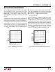
As the IN pin can withstand up to 80V, a high voltage
N-channel MOSFET can be used to protect the system
against rugged abuse from high transient or DC voltages
up to the BV
DSS
of the MOSFET. Figure 6 shows a 50V
input plugged into the LTC4361 controlling a 60V rated
MOSFET.
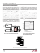
Input transients also occur when the current through the
cable inductance changes abruptly. This can happen when
the LTC4361 turns off the N-channel MOSFET rapidly in an
overvoltage or overcurrent event. Figure 7 shows an input
transient after an overcurrent. The current in L
IN
will cause
V
IN
to overshoot and avalanche the N-channel MOSFET to
C
OUT
. Typically, IN will be clamped to a voltage of V
OUT
+
1.3 • (BV
DSS
of Si1470DH) = 45V. This is well below the
85V absolute maximum voltage rating of the LTC4361.
The single, nonrepetitive, pulse of energy (E
AS
) absorbed
by the MOSFET during this avalanche breakdown with a
peak current I
AS
is approximated by the formula:
E
AS
= 0.5 • L
IN
• I
AS
2
For L
IN
= 0.7μH and I
AS
= 4A, then E
AS
= 5.6μJ. This is within
the I
AS
and E
AS
capabilities of most MOSFET’s including
the Si1470DH. So in most instances, the LTC4361 can
ride through such transients without a bypass capacitor,
transient voltage suppressor or other external components
at IN. Note that if an IN bypass capacitor is used, the V
IN
transients will overshoot less but last longer. If V
IN
dips
below V
IN(UVL)
for more than 10µs, the internal latch-off
latch in the LTC4361-1 could be inadvertently reset.
Figure 6. 50V Hot-Plug into the LTC4361
Figure 7. Overcurrent Turn-Off and Resulting Input Transient
V
IN
20V/DIV
V
OUT
1V/DIV
I
CABLE
5A/DIV
5µs/DIV
436112 F06
FDC5612
R
IN
= 150mΩ, L
IN
= 0.7µH
R
SENSE
= 25mΩ, LOAD = 10Ω, C
OUT
= 10µF
V
IN
20V/DIV
V
GATE
10V/DIV
V
OUT
5V/DIV
I
CABLE
5A/DIV
2µs/DIV
436112 F07
FIGURE 5 CIRCUIT
R
IN
= 150mΩ, L
IN
= 0.7µH
R
SENSE
= 25mΩ, LOAD = 10Ω, C
OUT
= 10µF