
Datasheet


LTC4361-1/LTC4361-2
6
436112fb
operaTion
Mobile devices like cell phones and MP3/MP4 players have
highly integrated subsystems fabricated from deep submi-
cron CMOS processes. The small form factor is accompanied
by low absolute maximum voltage ratings. The sensitive
electronics are susceptible to damage from transient or DC
overvoltage conditions from the power supply.
Failures or faults in the power adaptor can cause an overvolt-
age event. So can hot-plugging an AC adaptor into the power
input of the mobile device (see LT C Application Note 88).
Today’s mobile devices derive their power supply or recharge
their internal batteries from multiple alternative inputs like AC
wall adaptors, car battery adaptors and USB ports. A user
may unknowingly plug in the wrong adaptor, damaging the
device with a high or even a negative power supply voltage.
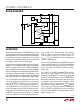
The LTC4361 protects low voltage electronics from these
overvoltage conditions by controlling a low cost external
N-channel MOSFET configured as a pass transistor. At
power-up (V
IN
> 2.1V), a start-up delay cycle begins. Any
overvoltage condition causes the delay cycle to continue
until a safe voltage is present. When the delay cycle com-
pletes, an internal high side switch driver slowly ramps up
the MOSFET gate, powering
up the output at a controlled
rate
and limiting the inrush current to the output capacitor.
If the voltage at the IN pin exceeds 5.8V (V
IN(OV)
),
GATE is pulled low quickly to protect the load. The
incoming power supply must remain below 5.7V
(V
IN(OV)
– ∆V
OV
) for the duration of the start-up delay to
restart the GATE ramp-up.
A sense resistor placed between IN and SENSE implements
an overcurrent protection with a 50mV trip threshold and
a 10µs glitch filter. After an overcurrent, the LTC4361-
1 latches off while the LTC4361-2 restarts following a
130ms delay.
The LTC4361 has a CMOS compatible ON input. When
driven low, the part is enabled. When driven high, the
external N-channel MOSFET is turned off and the supply
current of the LTC4361 drops to 1.5µA. The PWRGD pull-
down releases during this low current sleep mode, UVLO,
overvoltage or overcurrent and the subsequent 130ms
start-up delay. After the start-up delay, GATE starts its
slow ramp-up and ramps higher than V
GATE(TH)
to trigger
a 65ms delay cycle. When that completes, PWRGD pulls
low.The LTC4361 has a GATEP pin
that drives an optional
external
P-channel MOSFET to provide protection against
negative voltages at IN.
block Diagram
–
+
GND
436112 BD
10µA
ON
OUT
PWRGD
5.8V
500k
GATE
CONTROL
CHARGE
PUMP
OVERCURRENT
COMPARATOR
50mV
+
–
–
+
5.8V
5.7V
OVERVOLTAGE
COMPARATOR
IN SENSE
1.8M
200k
5.8V
GATEP
5µA
1V
+
–
V
GATE(TH)
GATE HIGH
COMPARATOR
+
–