
Datasheet


LTC4370
10
4370f
diverging, and so too, the supply currents. As the supply
voltages separate, the entire load current is steered to the
higher supply. Now, the servo command across the higher
supply’s MOSFET is folded back from the maximum to
the minimum servo to minimize power dissipated in the
MOSFET. The sharing capture range, ΔV
IN(SH)
, in Figure2a
is ±500mV, set by V
RANGE
. Figure 2b will be discussed
later in the MOSFET Selection section.
RANGE Pin Configuration
The RANGE pin resistor is decided by the design trade-off
between the sharing capture range and the power dissipated
in the MOSFET. A larger R
RANGE
increases the capture
range at the expense of enhanced power dissipation and
reduced load voltage. On the other hand, supplies with
tight tolerances can afford a smaller capture range and
therefore cooler operation of the MOSFETs.
As mentioned, the upper limit of the servo command ad-
justment is V
RANGE
plus the minimum forward regulation
voltage. Since an internal 10μA pull-up current flowing
through the external resistor sets V
RANGE
:
V
FR(MAX)
= 10µA • R
RANGE
+ V
FR(MIN)
(1)
If R
RANGE
is larger than 60k (including the pin open
state), the internal limit for the first term on the right-
hand
side of Equation 1 is 600mV, setting V
FR(MAX)
to
612mV or 625mV. Note that servo voltages nearing the
MOSFET’s body diode voltage may divert some or all cur-
rent to the diode especially at hot temperatures. This may
either cause FETON to go low if V
GS
falls below 0.7V, or
loss of sharing control. Also note that an open RANGE pin
biases itself to a voltage greater than 600mV.
Connecting the RANGE pin to V
CC
disables the load sharing
loop. The servo voltages for both MOSFETs are fixed at the
minimum with no adjustment. The device now behaves
as a dual ideal diode controller. This is handy for testing
purposes. Use the LTC4353 if only a dual ideal diode
controller is needed.
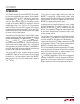
Power Supply Configuration
The LTC4370 can load share high side supplies down to
0V rail voltage. This requires powering the V
CC
pin with an
early external supply in the 2.9V to 6V range. In this range
of operation V
IN
should be lower than V
CC
. If V
CC
powers
up after V
IN
, and backfeeding of V
CC
by the internal 5V LDO
is a concern, then a series resistor (few 100Ω) or Schottky
diode
limits device power dissipation and backfeeding of
a low V
CC
supply when any V
IN
is high. A 0.1µF bypass
capacitor should also be connected between the V
CC
and
GND pins, close to the device. Figure 3 illustrates this.
If either V
IN
operates above 2.9V, then the external supply
at V
CC
is not needed. The 0.1µF capacitor is still required
for bypassing.
Start of Sharing
When currents are not being shared either because the
load current or one of the supplies is off, the COMP volt-
age is railed towards 0V or 2V depending on the input
signal to the error amplifier and its offset. For example,
applicaTions inForMaTion
Figure 3. Power Supply Configurations
GATE1
4370 F03
0V TO V
CC
0V TO
V
CC
V
IN1
V
CC
GATE2
V
IN2
LTC4370
2.9V TO 6V
GATE1
M1
M2
M1
M2
2.9V TO 18V
(0V TO 18V)
0V TO 18V
(2.9V TO 18V)
V
IN1
V
CC
GATE2
V
IN2
LTC4370
C
VCC
0.1µF
C
VCC
0.1µF
OPTIONAL
OR HERE