
Datasheet

LTC4370
14
4370f
Input Transient Protection
When the capacitances at the input and output are very
small, rapid changes in current can cause transients that
exceed the 24V absolute maximum rating of the V
IN
and
OUT pins. In ORing applications, one surge suppressor
connected from OUT to ground clamps all the inputs. In
the absence of a surge suppressor, an output capacitance
of 10μF is sufficient in most applications to prevent the
transient from exceeding 24V.
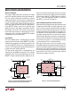
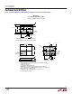
12V Design Example
This design example demonstrates the selection of
components in a 12V system with a 10A maximum load
current and ±2% tolerance supplies (Figure 6). That is
followed by the recalculations involved for a similar 5V
system (Figure 1).
First, calculate the R
DS(ON)
of the MOSFET to achieve
the desired forward drop at full load. Assuming a V
FWD
of 50mV:
R
DS(ON)
≤
V
FWD
I
LOAD
=
50mV
10A
= 5mΩ
The SUM85N03-06P offers a good solution in a DD-Pak
(TO-263) sized package with a 4.5mΩ R
DS(ON)
, 30V
BV
DSS
and 20V V
GS(MAX)
. Since 0.5I
L
• R
DS(ON)
is 22.5mV,
the servo amplifier will be able to regulate the 25mV mini-
mum forward regulation voltage leading to the maximum
possible sharing range set by V
RANGE
.
2% of 12V is 240mV. The sharing capture range, ΔV
IN(SH)
,
needs to be about 2× 240mV (±480mV) to work for most
supply voltage differences. A 47.5k R3 sets V
RANGE
to
475mV. Equation 1 is used to calculate the maximum
forward regulation voltage:
V
FR(MAX)
= 10µA • 47.5k + 25mV = 500mV
Equation 3 gives the maximum power dissipation in the
MOSFET to be:
P
D(MAX)
= 10A • 500mV = 5W
Sufficient PCB area with air flow needs to be provided
around the MOSFET drain to keep its junction temperature
below the 175°C maximum.
A 2.5mΩ sense resistor drops 25mV at full load and
yields an error amplifier offset induced sharing error of
2mV/(10A • 2.5mΩ) or 8% (Equation 4). At full load, the
sense resistor dissipates 10A
2
• 2.5mΩ or 250mW. Since
a 12V supply is large enough to tolerate a diode drop, fast
gate
turn-on is not needed. Hence, the CPO capacitor is
omitted. The input capacitance, C
ISS
, of the MOSFET is
about 3800pF. Since fast turn-on is not used, the COMP
capacitor C
C
can be just 10× C
ISS
at 0.039µF.
Red LED, D1, turns on when any one of the MOSFETs is
off, indicating a break in sharing. It requires around 3mA
for good luminous intensity. Accounting for a 2V diode
drop and 0.6V V
OL
, R4 is set to 2.7k.
5V Design Example
For a 5V, 10A system with ±3% tolerance supplies and
fast gate turn-on (Figure 1), the following components
need to be recalculated: R3, C1, C2, C
C
, and R4. R3 is
set to 30.1k to account for possible supply differences
(2 • 3% • 5V yields ±300mV). C1 and C2 are set to 10×
C
ISS
at 0.039µF. With fast turn-on, C
C
is selected closer
to 50× C
ISS
at 0.18µF. With the 5V supply, R4 needs to
be 820Ω to allow 3mA into the LED.
applicaTions inForMaTion