
Datasheet


LTC4415
4
4415fa
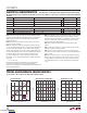
Typical perForMance characTerisTics
I-V Characteristics
On-Resistance vs Temperature
On-Resistance vs V
IN
T
A
= 25°C, V
IN1
= V
IN2
= 3.6V, R
CLIM
= 250Ω unless otherwise noted.
elecTrical characTerisTics
The l denotes the specifications which apply over the specified operating
junction temperature range, otherwise specifications are at T
A
= 25°C (Notes 2, 3). V
IN1
= V
IN2
= 3.6V, R
CLIM
= 250Ω, unless otherwise
specified.
SYMBOL PARAMETER CONDITIONS MIN TYP MAX UNITS
t
STAT(OFF)
STAT Turn-Off Time Disable to STAT Pull-Up 2 µs
t
WARN(ON)
WARN Turn-On Time Current Limit to WARN Pull-Down 500 µs
t
WARN(OFF)
WARN Turn-Off Time Out of Current Limit to WARN Pull-Up 5 µs
Enable Inputs (EN1, EN2)
V
ENTH
EN1 Rising and EN2 Falling Thresholds
l
760 800 840 mV
V
ENHYST
EN1 and EN2 Hysteresis 55 mV
Enable Pin Current When Pulled High V
EN1
= V
EN2
= 3.6V
l
0 1 µA
Note 1: Stresses beyond those listed under Absolute Maximum Ratings
may cause permanent damage to the device. Exposure to any Absolute
Maximum Rating condition for extended periods may affect device
reliability and lifetime.
Note 2: Unless otherwise specified, current into a pin is positive and
current out of a pin is negative.
Note 3: The LTC4415 is tested under pulsed load conditions such that
T
J
≈ T
A
. The LTC4415E is guaranteed to meet performance specifications
from 0°C to 85°C. Specifications over the –40°C to 125°C operating
junction temperature range are assured by design, characterization and
correlation with statistical process controls. The LTC4415I is guaranteed
over the full –40°C to 125°C operating junction temperature range.
The junction temperature (T
J
in °C) is calculated from the ambient
temperature (T
A
in °C) and power dissipation (P
D
in Watts) according to
the formula:
T
J
= T
A
+ (P
D
• θ
JA
)
Note that the maximum ambient temperature consistent with these
specifications is determined by specific operating conditions in
conjunction with board layout, the rated package thermal impedance and
other environmental factors.
Note 4: The LTC4415 includes overtemperature protection that is intended
to protect the device during momentary overload conditions. Junction
temperature will exceed 125°C when overtemperature protection is active.
Continuous operation above the specified maximum operating junction
temperature may impair device reliability.
Note 5: One channel enabled. Quiescent current is identical for each
channel.
Note 6: Enable inputs are driven to supply levels. Other diode is already
enabled so the chip bias circuits are active.
Note 7: Turn-on time is measured from enable to I
OUTx
rising through
1mA. When the output voltage is more than 1.2V, soft-start is disabled and
turn-on is faster.
Note 8: Current ramps from zero to the current limit during the soft-start
duration. Soft-start is measured from 10% to 90% of the current limit. If
the load condition is such that the current does not need to go up to the
current limit during start-up, the output voltage may reach steady state
sooner.
FORWARD VOLTAGE DROP (mV)
0
FORWARD CURRENT (A)
2
3
200
4415 G01
1
0
50
100
150
250
4
125°C
90°C
25°C
–40°C
R
CLIM
= 124Ω
TEMPERATURE (°C)
–50
20
R
ON
(mΩ)
30
40
50
60
0 50
100
150
4415 G02
70
80
–25 25
75
125
INPUT VOLTAGE (V)
1
20
R
ON
(mΩ)
30
40
50
60
70
80
2 3 4 5
4415 G03
6
Downloaded from Arrow.com.Downloaded from Arrow.com.Downloaded from Arrow.com.Downloaded from Arrow.com.