
Datasheet


LTC4415
9
4415fa
operaTion
The LTC4415 consists of two PowerPath ideal diode cir-
cuits within a single package. Each diode in the LTC4415
is capable of supplying a maximum rated output current of
4A from its input supply with typical forward conduction
resistance of 50mΩ.
The diodes are enabled using level-sensitive enable inputs
EN1 and EN2 with opposite polarity to achieve a prioritizer
function with minimal quiescent current during diode-OR
implementation. The enable threshold on the enable pins
(V
ENTH
) is 800mV (typical) with one-sided hysteresis of
55mV (typical). For rising voltage on the EN1 pin, Diode1
is enabled when V
EN1
> 800mV (typical), and on the fall-
ing edge it is disabled when V
EN1
< 745mV (typical). For
falling voltage on the EN2 pin, Diode 2 is enabled when
V
EN2
< 800mV (typical), and on the rising edge it is dis-
abled when V
EN1
> 855mV (typical). EN1 or EN2 pin volt-
ages should not exceed the highest voltage on the input
(IN1, IN2) or output (OUT1, OUT2) pins.
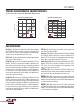
Forward conduction of the LTC4415 diodes has three op-
erating ranges as a function of the load current, as shown
in Figure 1 and described below:
1. For small load current, a low forward voltage drop
(V
FR
= 15mV typical) is maintained by modulating the
series resistance offered by the PFETs (P1/P2) in the
current paths as shown in the Block Diagram. This op-
erating mode is referred to as constant V
FR
regulation.
In battery-powered and low headroom applications, the
low forward drop of the ideal diodes extend the operat-
ing range beyond that of Schottky diodes.
2. At higher load currents, the LTC4415 gate driver can
no longer modulate the series resistance of the PFETs
(P1/P2) to maintain constant forward drop. This transi-
tion occurs when the gate voltage of the series PFETs
(P1/P2) has been brought down to GND. The ideal
diodes subsequently operate with constant resistance,
R
ON
, between inputs and outputs, IN1/IN2 and OUT1/
OUT2, respectively.
3. As the load current exceeds the current limit, the series
PFETs offer higher resistance between IN1/IN2 and
OUT1/OUT2 by reducing the gate drive in order to limit
the load current; so the forward voltage drop increases
rapidly. This operating mode is referred to as constant
current operation.
When the output of either diode is driven higher than its
input by an alternate supply, conduction through that diode
is suspended to prevent reverse conduction from OUT1/
OUT2 to IN1/IN2. This function allows implementation of
a power supply OR function by simply tying the outputs
OUT1 and OUT2 together.
Current Limit Setting
The output current limit of each diode can be set inde-
pendently by connecting resistors from the current limit
adjust pins CLIM1 and CLIM2 to ground. The current out
of the CLIM1 and CLIM2 pins are 1/1000 of the ideal diode
output currents I
OUT1
and I
OUT2
respectively. When the
load currents increase so that the CLIM1 or CLIM2 pin
voltages exceeds 0.5V, the LTC4415 detects an overcurrent
condition and regulates the current to a fixed value. The
required value of resistor R
CLIM
for output current limit
of I
LIM
is calculated as follows:
R
CLIM
=1000 •
0.5V
I
LIM
The allowed range of R
CLIM
is 125Ω to 1000Ω unless the
CLIM1/CLIM2 pins are shorted to GND, in which case
the LTC4415 limits the load current using a fixed internal
current limit of 6A.
Overcurrent Status
When either of the ideal diodes is operating in current
limit, the corresponding warning pin, WARN1/WARN2,
is pulled low by an open-drain NFET after a 500µs delay.
Normal operation resumes and the warning pin is released
CONSTANT CURRENT
CONSTANT
RESISTANCE
CONSTANT
VOLTAGE
FORWARD VOLTAGE (V)V
FR
4415 F01
CURRENT (A)
I
LIM
SLOPE =
1
R
ON
SLOPE =
1
R
FR
Figure 1. Forward Characteristics of LTC4415
Downloaded from Arrow.com.Downloaded from Arrow.com.Downloaded from Arrow.com.Downloaded from Arrow.com.Downloaded from Arrow.com.Downloaded from Arrow.com.Downloaded from Arrow.com.Downloaded from Arrow.com.Downloaded from Arrow.com.