
Datasheet


LTC4449
1
4449fa
n
4V to 6.5V V
CC
Operating Voltage
n
38V Maximum Input Supply Voltage
n
Adaptive Shoot-Through Protection
n
Rail-to-Rail Output Drivers
n
3.2A Peak Pull-Up Current
n
4.5A Peak Pull-Down Current
n
8ns TG Rise Time Driving 3000pF Load
n
7ns TG Fall Time Driving 3000pF Load
n
Separate Supply to Match PWM Controller
n
Drives Dual N-Channel MOSFETs
n
Undervoltage Lockout
n
Low Profi le (0.75mm) 2mm × 3mm DFN Package
TYPICAL APPLICATION
FEATURES
APPLICATIONS
DESCRIPTION
High Speed Synchronous
N-Channel MOSFET Driver
The LTC
®
4449 is a high frequency gate driver that
is designed to drive two N-Channel MOSFETs in a
synchronous DC/DC converter. The powerful rail-to-rail
driver capability reduces switching losses in MOSFETs
with high gate capacitance.
The LTC4449 features a separate supply for the input logic
to match the signal swing of the controller IC. If the input
signal is not being driven, the LTC4449 activates a shutdown
mode that turns off both external MOSFETs. The input logic
signal is internally level-shifted to the bootstrapped supply,
which functions at up to 42V above ground.
The LTC4449 contains undervoltage lockout circuits on
both the driver and logic supplies that turn off the external
MOSFETs when an undervoltage condition is present. An
adaptive shoot-through protection feature is also built-in
to prevent the power loss resulting from MOSFET cross-
conduction current.
The LTC4449 is available in the 2mm × 3mm DFN
package.
Synchronous Buck Converter Driver
n
Distributed Power Architectures
n
High Density Power Modules
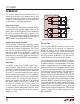
LTC4449 Driving 3000pF Capacitive Loads
TG
BOOST
V
IN
TO 38V
GND
TS
V
LOGIC
V
CC
LTC4449
BGPWM
V
CC
4V TO 6.5V
IN
V
OUT
4449 TA01a
TOP GATE
(TG - TS)
5V/DIV
INPUT (IN)
5V/DIV
4449 TA01b
BOTTOM GATE
(BG) 5V/DIV
10ns/DIV
L, LT, LTC, LTM, Linear Technology and the Linear logo are registered trademarks of Linear
Technology Corporation. All other trademarks are the property of their respective owners.