
Datasheet


LTC4449
8
4449fa
OPERATION
Rise/Fall Time
Since the power MOSFETs generally account for the
majority of power loss in a converter, it is important to
quickly turn them on and off, thereby minimizing the
transition time and power loss. The LTC4449’s peak pull-
up current of 3.2A for both BG and TG produces a rapid
turn-on transition for the MOSFETs. This high current is
capable of driving a 3nF load with an 8ns rise time.
It is also important to turn the power MOSFETs off quickly
to minimize power loss due to transition time; however,
an additional benefi t of a strong pull-down on the driver
outputs is the prevention of cross-conduction current. For
example, when BG turns the low side power MOSFET off and
TG turns the high side power MOSFET on, the voltage on
the TS pin will rise to V
IN
very rapidly. This high frequency
positive voltage transient will couple through the C
GD
capacitance of the low side power MOSFET to the BG pin.
If the BG pin is not held down suffi ciently, the voltage on
the BG pin will rise above the threshold voltage of the low
side power MOSFET, momentarily turning it back on. As
a result, both the high side and low side MOSFETs will be
conducting, which will cause signifi cant cross-conduction
current to fl ow through the MOSFETs from V
IN
to ground,
thereby introducing substantial power loss. A similar effect
occurs on TG due to the C
GS
and C
GD
capacitances of the
high side MOSFET.
The hysteresis between the corresponding V
IH
and V
IL
voltage levels eliminates false triggering due to noise
during switch transitions; however, care should be taken
to keep noise from coupling into the IN pin, particularly
in high frequency, high voltage applications.
Undervoltage Lockout
The LTC4449 contains undervoltage lockout detectors that
monitor both the V
CC
and V
LOGIC
supplies. When V
CC
falls
below 3.04V or V
LOGIC
falls below 2.65V, the output pins
BG and TG are pulled to GND and TS, respectively. This
turns off both of the external MOSFETs. When V
CC
and
V
LOGIC
have adequate supply voltage for the LTC4449 to
operate reliably, normal operation will resume.
Adaptive Shoot-Through Protection
Internal adaptive shoot-through protection circuitry
monitors the voltages on the external MOSFETs to ensure
that they do not conduct simultaneously. The LTC4449
does not allow the bottom MOSFET to turn on until the
gate-source voltage on the top MOSFET is suffi ciently
low, and vice-versa. This feature improves effi ciency by
eliminating cross-conduction current from fl owing from
the V
IN
supply through the MOSFETs to ground during a
switch transition.
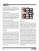
Output Stage
A simplifi ed version of the LTC4449’s output stage is
shown in Figure 2. The pull-up device on both the BG and
TG outputs is an NPN bipolar junction transistor (Q1 and
Q2) in parallel with a low resistance P-channel MOSFET
(P1 and P2). This powerful combination rapidly pulls the
BG and TG outputs to their positive rails (V
CC
and BOOST,
respectively). Both BG and TG have N-channel MOSFET
pull-down devices (N1 and N2) which pull BG and TG
down to their negative rails, GND and TS. An additional
NPN bipolar junction transistor (Q3) is present on BG
to increase its pull-down drive current capacity. The
rail-to-rail voltage swing of the BG and TG output pins
is important in driving external power MOSFETs, whose
R
DS(ON)
is inversely proportional to its gate overdrive
voltage (V
GS
– V
TH
).
BOOST
LTC4449
TG
TS
C
GS
C
GD
HIGH SIDE
POWER
MOSFET
V
IN
V
CC
BG
N2
P2
Q2
GND
C
GS
4449 F02
C
GD
LOW SIDE
POWER
MOSFET
LOAD
INDUCTOR
Q3
N1
P1
Q1
Figure 2. Capacitance Seen by BG and TG During Switching