
Datasheet
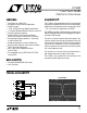


3
LTC485
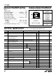
SYMBOL PARAMETER CONDITIONS MIN TYP MAX UNITS
t
PLH
Driver Input to Output R
DIFF
= 54Ω, C
L1
= C
L2
= 100pF, ● 10 30 50 ns
t
PHL
Driver Input to Output
(Figures 3 and 5)
● 10 30 50 ns
t
SKEW
Driver Output to Output ● 510ns
t
r
, t
f
Driver Rise or Fall Time ● 31525ns
t
ZH
Driver Enable to Output High C
L
= 100pF (Figures 4 and 6) S2 Closed ● 40 70 ns
t
ZL
Driver Enable to Output Low C
L
= 100pF (Figures 4 and 6) S1 Closed ● 40 70 ns
t
LZ
Driver Disable Time from Low C
L
= 15pF (Figures 4 and 6) S1 Closed ● 40 70 ns
t
HZ
Driver Disable Time from High C
L
= 15pF (Figures 4 and 6) S2 Closed ● 40 70 ns
t
PLH
Receiver Input to Output R
DIFF
= 54Ω, C
L1
= C
L2
= 100pF, ● 30 90 200 ns
t
PHL
(Figures 3 and 7)
● 30 90 200 ns
t
SKD
t
PLH
– t
PHL
Differential Receiver Skew ● 13 ns
t
ZL
Receiver Enable to Output Low C
RL
= 15pF (Figures 2 and 8) S1 Closed ● 20 50 ns
t
ZH
Receiver Enable to Output High C
RL
= 15pF (Figures 2 and 8) S2 Closed ● 20 50 ns
t
LZ
Receiver Disable from Low C
RL
= 15pF (Figures 2 and 8) S1 Closed ● 20 50 ns
t
HZ
Receiver Disable from High C
RL
= 15pF (Figures 2 and 8) S2 Closed ● 20 50 ns
SWITCHI G CHARACTERISTICS
U
V
CC
= 5V ±5%, unless otherwise noted. (Notes 2 and 3)
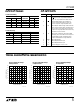
3V
DE
A
B
DI
R
DIFF
C
L1
C
L2
RO
15pF
A
B
RE
LTC485 • F03
OUTPUT
UNDER TEST
C
L
S1
S2
V
CC
500Ω
LTC485 • F02
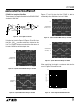
Figure 3. Driver/Receiver Timing Test Circuit Figure 4. Driver Timing Test Load #2
RECEIVER
OUTPUT
C
RL
15pF
1k
S1
S2
TEST POINT
V
CC
1k
LTC485 • F02
V
OD
A
B
R
R
V
OC
LTC485 • F01
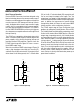
Figure 1. Driver DC Test Load Figure 2. Receiver Timing Test Load
The ● denotes specifications which apply over the full operating
temperature range.
Note 1: Absolute maximum ratings are those beyond which the safety of
the device cannot be guaranteed.
Note 2: All currents into device pins are positive; all currents out ot device
pins are negative. All voltages are referenced to device ground unless
otherwise specified.
Note 3: All typicals are given for V
CC
= 5V and T
A
= 25°C.
Note 4: The LTC485 is guaranteed by design to be functional over a supply
voltage range of 5V ±10%. Data sheet parameters are guaranteed over the
tested supply voltage range of 5V ±5%.
TEST CIRCUITS