
Datasheet


5
LTC485
CCHARA TERIST
ICS
UW
AT
Y
P
I
CA
LPER
F
O
R
C
E
LTC485 Transmitting
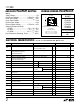
INPUTS OUTPUTS
RE DE DI B A
X 1 1 No Fault 0 1
X 1 0 No Fault 1 0
X0X X ZZ
X 1 X Fault Z Z
LINE
CONDITION
LTC485 Receiving
INPUTS OUTPUTS
RE DE A – B R
00≥0.2V 1
00≤–0.2V 0
0 0 Inputs Open 1
10 X Z
PIN # NAME DESCRIPTION
1 RO Receiver Output. If the receiver output is enabled
(RE low), then if A > B by 200mV, RO will be
high. If A < B by 200mV, then RO will be low.
2 RE Receiver Output Enable. A low enables the
receiver output, RO. A high input forces the
receiver output into a high impedance state.
3 DE Driver Outputs Enable. A high on DE enables the
driver output. A and B, and the chip will function
as a line driver. A low input will force the driver
outputs into a high impedance state and the chip
will function as a line receiver.
4 DI Driver Input. If the driver outputs are enabled
(DE high), then a low on DI forces the outputs A
low and B high. A high on DI with the driver
outputs enabled will force A high and B low.
5 GND Ground Connection.
6 A Driver Output/Receiver Input.
7 B Driver Output/Receiver Input.
8V
CC
Positive Supply; 4.75 < V
CC
< 5.25
PI FU CTIO S
UU U
FU CTIO TABLES
UU
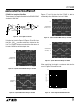
Receiver Output High Voltage
vs Output Current
Receiver Output Low Voltage
vs Output Current
OUTPUT VOLTAGE (V)
0
0
OUTPUT CURRENT (mA)
4
12
16
20
1.0
36
LTC485 • TPC01
8
0.5 2.0
24
28
32
1.5
T
A
= 25°C
OUTPUT VOLTAGE (V)
5
0
OUTPUT CURRENT (mA)
–2
–6
–8
–10
3
–18
LTC485 • TPC02
–4
4
–12
–14
–16
2
T
A
= 25°C
TEMPERATURE (°C)
–50
3.0
OUTPUT VOLTAGE (V)
3.2
3.6
3.8
4.0
75
4.8
LTC485 • TPC03
3.4
0 125
4.2
4.4
4.6
–25
25 50
100
I = 8mA
Receiver Output High Voltage
vs Temperature