
Datasheet

LTC485
3
485fk
For more information www.linear.com/LTC485
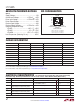
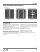
ELECTRICAL CHARACTERISTICS
Note 1: Stresses beyond those listed under Absolute Maximum Ratings
may cause permanent damage to the device. Exposure to any Absolute
Maximum Rating condition for extended periods may affect device
reliability and lifetime.
Note 2: All currents into device pins are positive; all currents out ot device
pins are negative. All voltages are referenced to device ground unless
otherwise specified.
The l denotes the specifications which apply over the full operating
temperature range, otherwise specifications are at T
A
= 25°C. V
CC
= 5V ±5%, unless otherwise noted. (Notes 2 and 3)
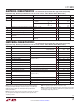
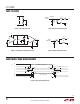
SWITCHING CHARACTERISTICS
The l denotes the specifications which apply over the full operating
temperature range, otherwise specifications are at T
A
= 25°C. V
CC
= 5V ±5%, unless otherwise noted. (Notes 2 and 3)
SYMBOL PARAMETER CONDITIONS MIN TYP MAX UNITS
I
CC
Supply Current No Load, Pins 2, 3, 4 = 0V or 5V Outputs Enabled
Outputs Disabled
l
l
500
300
900
500
μA
μA
I
OSD1
Driver Short-Circuit Current, V
OUT
= HIGH V
O
= – 7V
l
35 100 250 mA
I
OSD2
Driver Short-Circuit Current, V
OUT
= LOW V
O
= 10V
l
35 100 250 mA
I
OSR
Receiver Short-Circuit Current 0V ≤ V
O
≤ V
CC
l
7 85 mA
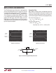
t
PLH
Driver Input to Output R
DIFF
= 54Ω, C
L1
= C
L2
= 100pF,
(Figures 3 and 5)
l
10 30 50 ns
t
PHL
Driver Input to Output
l
10 30 50 ns
t
SKEW
Driver Output to Output
l
5 10 ns
t
r
, t
f
Driver Rise or Fall Time
l
3 15 25 ns
t
ZH
Driver Enable to Output High C
L
= 100pF (Figures 4 and 6) S2 Closed
l
40 70 ns
t
ZL
Driver Enable to Output Low C
L
= 100pF (Figures 4 and 6) S1 Closed
l
40 70 ns
t
LZ
Driver Disable Time from Low C
L
= 15pF (Figures 4 and 6) S1 Closed
l
40 70 ns
t
HZ
Driver Disable Time from High C
L
= 15pF (Figures 4 and 6) S2 Closed
l
40 70 ns
t
PLH
Receiver Input to Output R
DIFF
= 54Ω, CL1 = CL2 = 100pF,
(Figures 3 and 7)
l
30 90 200 ns
t
PHL
l
30 90 200 ns
t
SKD
|t
PLH
– t
PHL
| Differential Receiver Skew
l
13 ns
t
ZL
Receiver Enable to Output Low C
RL
= 15pF (Figures 2 and 8) S1 Closed
l
20 50 ns
t
ZH
Receiver Enable to Output High C
RL
= 15pF (Figures 2 and 8) S2 Closed
l
20 50 ns
t
LZ
Receiver Disable from Low C
RL
= 15pF (Figures 2 and 8) S1 Closed
l
20 50 ns
t
HZ
Receiver Disable from High C
RL
= 15pF (Figures 2 and 8) S2 Closed
l
20 50 ns
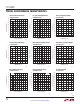
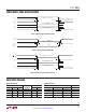
SYMBOL PARAMETER CONDITIONS MIN TYP MAX UNITS
V
IL
Input Low Voltage DE, DI, RE
l
0.8 V
I
IN1
Input Current DE, DI, RE
l
±2 μA
I
IN2
Input Current (A, B) DE = 0, V
CC
= 0V or 5.25V V
IN
= 12V
C-, I-Grade
V
IN
= –7V
l
l
1
–0.8
mA
mA
M-Grade
V
IN
= 12V
V
IN
= –7V
l
l
2
–1.6
mA
mA
V
TH
Differential Input Threshold Voltage for Receiver –7V ≤ V
CM
≤ 12V
l
–0.2 0.2 V
ΔV
TH
Receiver Input Hysteresis V
CM
= 0V
l
70 mV
V
OH
Receiver Output High Voltage I
O
= –4mA, V
ID
= 200mV
l
3.5 V
V
OL
Receiver Output Low Voltage I
O
= 4mA, V
ID
= –200mV
l
0.4 V
I
OZR
Three-State (High Impedance) Output Current
at Receiver
V
CC
= Max, 0.4V ≤ V
O
≤ 2.4V
l
±1 μA
R
IN
Receiver Input Resistance –7V ≤ V
CM
≤ 12V (C-, I-Grade)
(M-Grade)
l
l
12
6
kΩ
kΩ
Note 3: All typicals are given for V
CC
= 5V and T
A
= 25°C.
Note 4: The LTC485 is guaranteed by design to be functional over a supply
voltage range of 5V ±10%. Data sheet parameters are guaranteed over the
tested supply voltage range of 5V ±5%.