
Datasheet

LTC485
5
485fk
For more information www.linear.com/LTC485
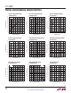
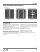
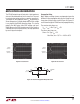
TYPICAL PERFORMANCE CHARACTERISTICS
Receiver |t
PLH
– t
PHL
|
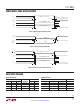
vs Temperature Driver Skew vs Temperature Supply Current vs Temperature
TEMPERATURE (°C)
–50
3.0
TIME (ns)
3.5
4.5
5.0
5.5
75
7.5
485 G10
4.0
0 125
6.0
6.5
7.0
–25
25 50
100
TEMPERATURE (°C)
–50
0
TIME (ns)
0.6
1.8
2.4
3.0
75
5.4
485 G11
1.2
0 125
3.6
4.2
4.8
–25
25 50
100
TEMPERATURE (°C)
–50
100
SUPPLY CURRENT (µA)
160
280
340
400
75
640
485 G12
220
0 125
460
520
580
–25
25 50
100
DRIVER ENABLED
DRIVER DISABLED
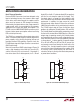
PIN FUNCTIONS
RO (Pin 1): Receiver Output. If the receiver output is en-
abled (RE low), then if A > B by 200mV, RO will be high.
If A < B by 200mV, then RO will be low
.
RE (Pin 2): Receiver Output Enable. A low enables the
receiver output, RO. A high input forces the receiver output
into a high impedance state.
DE (Pin 3): Driver Output Enable. A high on DE enables
the driver outputs, A and B, and the chip will function as
a line driver. A low input will force the driver outputs into
a high impedance state and the chip will function as a
line receiver.
DI (Pin 4): Driver Input. If the driver outputs are enabled
(DE high), then a low on DI forces the outputs A low and
B high. A high on DI with the driver outputs enabled will
force A high and B low.
GND (Pin 5): Ground Connection.
A (Pin 6): Driver Output/Receiver Input.
B (Pin 7): Driver Output/Receiver Input.
V
CC
(Pin 8): Positive Supply; 4.75 < V
CC
< 5.25.