
Datasheet


LTC486
3
486fc
DC ELECTRICAL CHARACTERISTICS
V
CC
= 5V ±5%, 0°C ≤ Temperature ≤ 70°C (Commercial), –40°C ≤ Temperature ≤ 85°C (Industrial) (Notes 2, 3)
SYMBOL PARAMETER CONDITIONS MIN TYP MAX UNITS
V
OD1
Differential Driver Output Voltage (Unloaded) I
OUT
= 0 5 V
V
OD2
Differential Driver Output Voltage (With Load) R = 50Ω; (RS422) 2 V
R = 27Ω; (RS485) (Figure 1) 1.5 5 V
V
OD
Change in Magnitude of Driver Differential
Output Voltage for Complementary Output States
R = 27Ω or R = 50Ω
(Figure 1)
0.2 V
V
OC
Driver Common-Mode Output Voltage 3 V
|V
OC
| Change in Magnitude of Driver Common-Mode
Output Voltage for Complementary Output States
0.2 V
V
IH
Input High Voltage DI, EN, EN 2.0 V
V
IL
Input Low Voltage 0.8 V
I
IN1
Input Current ±2 µA
I
CC
Supply Current No Load Output Enabled
Output Disabled
110
110
200
200
µA
µA
I
OSD1
Driver Short-Circuit Current, V
OUT
= High V
OUT
= –7V 100 250 mA
I
OSD2
Driver Short-Circuit Current, V
OUT
= Low V
OUT
= 12V 100 250 mA
I
OZ
High Impedance State Output Current V
OUT
= –7V to 12V ±10 ±200 µA
SWITCHING CHARACTERISTICS
V
CC
= 5V ±5%, 0°C ≤ Temperature ≤ 70°C (Commercial), –40°C ≤ Temperature ≤ 85°C (Industrial) (Notes 2, 3)
SYMBOL PARAMETER CONDITIONS MIN TYP MAX UNITS
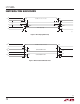
t
PLH
Driver Input to Output R
DIFF
= 54Ω, C
L1
= C
L2
= 100pF
(Figures 2, 4)
10 30 50 ns
t
PHL
Driver Input to Output 10 30 50 ns
t
SKEW
Driver Output to Output 5 15 ns
t
r
, t
f
Driver Rise or Fall Time 5 15 25 ns
t
ZH
Driver Enable to Output High C
L
= 100pF (Figures 3, 5) S2 Closed 35 70 ns
t
ZL
Driver Enable to Output Low C
L
= 100pF (Figures 3, 5) S1 Closed 35 70 ns
t
LZ
Driver Disable Time from Low C
L
= 15pF (Figures 3, 5) S1 Closed 35 70 ns
t
HZ
Driver Disable Time from High C
L
= 15pF (Figures 3, 5) S2 Closed 35 70 ns
Note 1: Stresses beyond those listed under Absolute Maximum Ratings
may cause permanent damage to the device. Exposure to any Absolute
Maximum Rating condition for extended periods may affect device
reliability and lifetime.
Note 2: All currents into device pins are positive; all currents out of device
pins are negative. All voltages are referenced to device ground unless
otherwise specified.
Note 3: All typicals are given for V
CC
= 5V and temperature = 25°C.