
Datasheet


LTC488/LTC489
1
4889fb
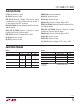
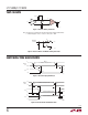
TYPICAL APPLICATION
DESCRIPTION
Quad RS485 Line Receiver
The LTC
®
488 and LTC489 are low power differential bus/
line receivers designed for multipoint data transmission
standard RS485 applications with extended common
mode range (12V to –7V). They also meet the require-
ments of RS422.
The CMOS design offers signifi cant power savings over
its bipolar counterpart without sacrifi cing ruggedness
against overload or ESD damage.
The receiver features three-state outputs, with the receiver
output maintaining high impedance over the entire com-
mon mode range.
The receiver has a fail-safe feature which guarantees a
high output state when the inputs are left open.
Both AC and DC specifi cations are guaranteed 4.75V to
5.25V supply voltage range.
L, LT, LTC and LTM are registered trademarks of Linear Technology Corporation. All other
trademarks are the property of their respective owners.
FEATURES
APPLICATIONS
n
Low Power: I
CC
= 7mA Typ
n
Designed for RS485 or RS422 Applications
n
Single 5V Supply
n
–7V to 12V Bus Common Mode Range Permits ±7V
Ground Difference Between Devices on the Bus
n
60mV Typical Input Hysteresis
n
Receiver Maintains High Impedance in Three-State or
with the Power Off
n
28ns Typical Receiver Propagation Delay
n
Pin Compatible with the SN75173 (LTC488)
n
Pin Compatible with the SN75175 (LTC489)
n
Low Power RS485/RS422 Receivers
n
Level Translator
120Ω
4000 FT 24 GAUGE TWISTED PAIR
DI
RECEIVER
1/4 LTC488
120Ω
DRIVER
1/4 LTC486
RO
EN
EN
1
2
4
12
3
EN
EN
120Ω
4000 FT 24 GAUGE TWISTED PAIR
DI
RECEIVER
1/4 LTC489
120Ω
DRIVER
1/4 LTC487
RO
EN12
1
2
4
3
EN12
4889 TA01