
Datasheet


LTC488/LTC489
6
4889fb
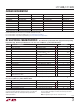
TEST CIRCUITS
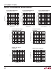
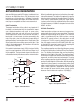
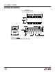
SWITCHING TIME WAVEFORMS
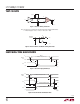
Figure 1. Receiver Timing Test Circuit
Note: The input pulse is supplied by a generator having the following characteristics:
f = 1MHz, Duty Cycle = 50%, t
r
< 10ns, t
f
≤ 10ns, Z
OUT
= 50Ω
Figure 2. Receiver Enable and Disable Timing Test Circuit
D
4889 F01
DRIVER RECEIVER
C
L
RO
A
B
54Ω
100pF
100pF
1k
4889 F02
C
L
S1
S2
1k
V
CC
RECEIVER
OUTPUT
0V
–V
OD2
t
PHL
f = 1MHz; t
r
≤ 10ns; t
f
≤ 10ns
0V
t
PLH
V
OD2
INPUT
A, B
V
OH
1.5V
1.5V
V
OL
RO
INPUT
4889 F03
f = 1MHz; t
r
≤ 10ns; t
f
≤ 10ns
1.5V
RO
4889 F04
0V
3V
1.5V
t
ZL
V
OL
V
OH
1.5V
t
LZ
0.5V
0.5V
t
HZ
OUTPUT NORMALLY LOW
OUTPUT NORMALLY HIGH
0V
5V
1.5V
t
ZH
RO
EN OR
EN12
Figure 3. Receiver Propagation Delays
Figure 4. Receiver Enable and Disable Times