
Datasheet


3
LTC490
490fb
Note 1: Absolute maximum ratings are those beyond which the safety of
the device cannot be guaranteed.
Note 2: All currents into device pins are positive; all currents out of device
pins are negative. All voltages are referenced to device ground unless
otherwise specified.
Note 3: All typicals are given for V
CC
= 5V and Temperature = 25°C.
SYMBOL PARAMETER CONDITIONS MIN TYP MAX UNITS
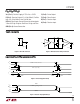
t
PLH
Driver Input to Output R
DIFF
= 54Ω, C
L1
= C
L2
= 100pF (Figures 2, 3)
●
10 30 50 ns
t
PHL
Driver Input to Output R
DIFF
= 54Ω, C
L1
= C
L2
= 100pF (Figures 2, 3)
●
10 30 50 ns
t
SKEW
Driver Output to Output R
DIFF
= 54Ω, C
L1
= C
L2
= 100pF (Figures 2, 3)
●
5ns
t
r
, t
f
Driver Rise or Fall Time R
DIFF
= 54Ω, C
L1
= C
L2
= 100pF (Figures 2, 3)
●
5525 ns
t
PLH
Receiver Input to Output R
DIFF
= 54Ω, C
L1
= C
L2
= 100pF (Figures 2, 4)
●
40 70 150 ns
t
PHL
Receiver Input to Output R
DIFF
= 54Ω, C
L1
= C
L2
= 100pF (Figures 2, 4)
●
40 70 150 ns
t
SKD
t
PLH
– t
PHL
Differential Receiver Skew R
DIFF
= 54Ω, C
L1
= C
L2
= 100pF (Figures 2, 4)
●
13 ns
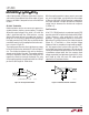
SWITCHI G CHARACTERISTICS
U
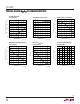
Driver Output High Voltage Driver Differential Output Voltage Driver Output Low Voltage
vs Output Current vs Output Current vs Output Current
TYPICAL PERFOR A CE CHARACTERISTICS
UW
OUTPUT VOLTAGE (V)
0
OUTPUT CURRENT (mA)
0
–24
– 4 8
–72
–96
1234
LTC490 • TPC01
T
A
= 25°C
OUTPUT VOLTAGE (V)
0
OUTPUT CURRENT (mA)
0
16
32
48
64
1234
LTC490 • TPC02
T
A
= 25°C
OUTPUT VOLTAGE (V)
0
OUTPUT CURRENT (mA)
0
20
40
60
80
1234
LTC490 • TPC03
T
A
= 25°C
The ● denotes the specificatiions which apply over the full
operating temperature range, otherwise specifications are at T
A
= 25°C. V
CC
= 5V ±5%